Design Considerations
Stratix II and Stratix II GX on-chip series and parallel termination
provides the convenience of no external components. External pull-up
resistors can be used to terminate the voltage-referenced I/O standards
such as SSTL-2 and HSTL.
1
Refer to the “Stratix II and Stratix II GX I/O Standards Support”
on page 4–2 for more information on the termination scheme of
various single-ended I/O standards.
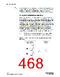
Differential I/O Standards
Differential I/O standards typically require a termination resistor
between the two signals at the receiver. The termination resistor must
match the differential load impedance of the bus. Stratix II and
Stratix II GX devices provide an optional differential on-chip resistor
when using LVDS and HyperTransport standards.
I/O Banks Restrictions
Each I/O bank can simultaneously support multiple I/O standards. The
following sections provide guidelines for mixing non-voltage-referenced
and voltage-referenced I/O standards in Stratix II and Stratix II GX
devices.
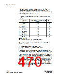
Non-Voltage-Referenced Standards
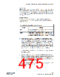
Each Stratix II and Stratix II GX device I/O bank has its own VCCIO pins
and supports only one VCCIO, either 1.5, 1.8, 2.5, or 3.3 V. An I/O bank can
simultaneously support any number of input signals with different I/O
standard assignments, as shown in Table 4–8.
For output signals, a single I/O bank supports non-voltage-referenced
output signals that are driving at the same voltage as VCCIO. Since an I/O
bank can only have one VCCIO value, it can only drive out that one value
for non-voltage-referenced signals. For example, an I/O bank with a
2.5-V VCCIO setting can support 2.5-V standard inputs and outputs and
3.3-V LVCMOS inputs (not output or bidirectional pins).
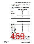
Table 4–8. Acceptable Input Levels for LVTTL and LVCMOS (Part 1 of 2)
Acceptable Input Levels (V)
Bank VCCIO
(V)
3.3
v
v
2.5
v (1)
v
1.8
1.5
3.3
2.5
4–34
Stratix II Device Handbook, Volume 2
Altera Corporation
January 2008

 ALTERA [ ALTERA CORPORATION ]