Conclusion
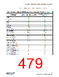
Table 4–10. Stratix II and Stratix II GX I/O Standard DC Current Specification (Part 2 of 2)
Note (1)
IPIN (mA), Left and Right I/O
I
PIN (mA), Top and Bottom I/O Banks
I/O Standard
Banks(2)
Notes to Table 4–10:
(1) The current value obtained for differential HSTL and differential SSTL standards is per pin and not per differential
pair, as opposed to the per-pair current value of LVDS and HyperTransport standards.
(2) This does not apply to the right I/O banks of Stratix II GX devices. Stratix II GX devices have transceivers on the
right I/O banks.
(3) The DC power specification of each I/O standard depends on the current sourcing and sinking capabilities of the
I/O buffer programmed with that standard, as well as the load being driven. LVTTL, LVCMOS, 2.5-V, 1.8-V, and
1.5-V outputs are not included in the static power calculations because they normally do not have resistor loads in
real applications. The voltage swing is rail-to-rail with capacitive load only. There is no DC current in the system.
(4) This IPIN value represents the DC current specification for the default current strength of the I/O standard. The IPIN
varies with programmable drive strength and is the same as the drive strength as set in Quartus II software. Refer
to the Stratix II Architecture chapter in volume 1 of the Stratix II Device Handbook or the Stratix II GX Architecture
chapter in volume 1 of the Stratix II GX Device Handbook for a detailed description of the programmable drive
strength feature of voltage-referenced I/O standards.
Table 4–10 only shows the limit on the static power consumed by an I/O
standard. The amount of power used at any moment could be much
higher, and is based on the switching activities.
Stratix II and Stratix II GX devices provide I/O capabilities that allow
Conclusion
you to work in compliance with current and emerging I/O standards and
requirements. With the Stratix II or Stratix II GX devices features, such as
programmable driver strength, you can reduce board design interface
costs and increase the development flexibility.
Refer to the following references for more information:
References
■
■
Interface Standard for Nominal 3V/ 3.3-V Supply Digital Integrated
Circuits, JESD8-B, Electronic Industries Association, September 1999.
2.5-V +/- 0.2V (Normal Range) and 1.8-V to 2.7V (Wide Range)
Power Supply Voltage and Interface Standard for Non-terminated
Digital Integrated Circuits, JESD8-5, Electronic Industries
Association, October 1995.
■
■
1.8-V +/- 0.15 V (Normal Range) and 1.2 V - 1.95 V (Wide Range)
Power Supply Voltage and Interface Standard for Non-terminated
Digital Integrated Circuits, JESD8-7, Electronic Industries
Association, February 1997.
1.5-V +/- 0.1 V (Normal Range) and 0.9 V - 1.6 V (Wide Range) Power
Supply Voltage and Interface Standard for Non-terminated Digital
Integrated Circuits, JESD8-11, Electronic Industries Association,
October 2000.
4–42
Stratix II Device Handbook, Volume 2
Altera Corporation
January 2008

 ALTERA [ ALTERA CORPORATION ]