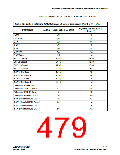
Selectable I/O Standards in Stratix II and Stratix II GX Devices
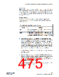
Table 4–10 shows the I/O standard DC current specification.
Table 4–10. Stratix II and Stratix II GX I/O Standard DC Current Specification (Part 1 of 2)
Note (1)
I
PIN (mA), Left and Right I/O
IPIN (mA), Top and Bottom I/O Banks
I/O Standard
Banks(2)
LVTTL
LVCMOS
2.5 V
(3)
(3)
(3)
(3)
(3)
(3)
1.8 V
(3)
(3)
1.5 V
(3)
(3)
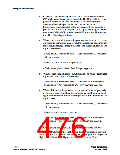
3.3-V PCI
1.5
NA
NA
12 (4)
16 (4)
10 (4)
NA
12
3.3-V PCI-X
1.5
SSTL-2 Class I
12 (4)
24 (4)
12 (4)
20 (4)
12 (4)
20 (4)
12 (4)
20 (4)
12
SSTL-2 Class II
SSTL-18 Class I
SSTL-18 Class II
1.8-V HSTL Class I
1.8-V HSTL Class II
NA
8
1.5-V HSTL Class I
1.5-V HSTL Class II
NA
12
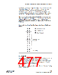
Differential SSTL-2 Class I
Differential SSTL-2 Class II
Differential SSTL-18 Class I
Differential SSTL-18 Class II
1.8-V differential HSTL Class I
1.8-V differential HSTL Class II
1.5-V differential HSTL Class I
1.5-V differential HSTL Class II
24
16
12
10
20
NA
12
12
20
NA
8
12
20
NA
Altera Corporation
January 2008
4–41
Stratix II Device Handbook, Volume 2

 ALTERA [ ALTERA CORPORATION ]