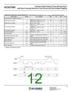
Isolated, Digital Output, Power Monitoring IC
with Zero-Crossing Detection, Overcurrent and Overvoltage Flagging
ACS37800
When bypass_n_en = 1, it is important to define the number of
Configurable Settings
samples used to calculate RMS. This can be done in the field
n. The field n is the number of 32 kHz samples that are used to
calculate the RMS. The minimum effective n that is used when
calculating RMS is 4. If a value of less than 4 is chosen for n,
then 4 is internally used. The first useable RMS calculation on
start up with bypass_n_en = 1 is after 2 × n samples.
PHASE DELAY
Phase delay may be introduced on either the voltage or current
channel to account for known phase delay at other points in the
system using the ichan_del_en and chan_ del_sel fields. ichan_
del_en determines if the voltage channel or current channel will
be delayed. The chosen channel will be delayed by the configured
amount in chan_del_sel, up to 5° of delay.
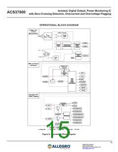
Configuring the DIO Pins (I2C Devices)
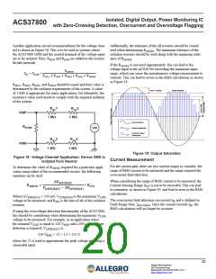
AVERAGING CHANNEL
FLAGS TO BE ROUTED TO THE DIO PINS
The ACS37800 contains two averaging paths. VRMS, IRMS, and
PACTIVE can be routed to these average blocks as shown in Figure 8
using iavgselen and pavgselen.
When the device is configured to be in I2C mode (comm_sel in
EEPROM = 1), pins 9 and 10 become digital I/O pins, DIO_1
and DIO_0, respectively. The digital I/O pins are low true, mean-
ing that a voltage below the DIO Output Low Level maximum
(VOL(DIO)max) is to be interpreted as logic 1 and a voltage above
DIO Output High Level minimum (VOH(DIO)min) is to be inter-
preted as a logic 0. The Digital I/O pins can be configured in
EEPROM to represent the following functions:
AVERAGING TIME
Each averaging path on the ACS37800 consists of two averag-
ing blocks that each allow for a configurable number of averages
based on the EEPROM fields rms_avg_1 and rms_avg_2.
The output of the first averaging block feeds into the input of the
second averaging block. The output of each block is accessible
for each channel.
DIO_O
dio_0_sel value (EEPROM)
Function
OVERVOLTAGE AND UNDERVOLTAGE DETECTION
FOR VRMS
0
1
2
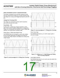
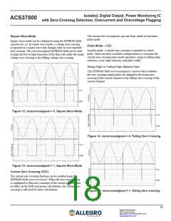
ZC: zero crossing
ovrms: the VRMS overvoltage flag
uvrms: The VRMS undervoltage flag
This device has programmable overvoltage and undervoltage
RMS flags that will signal when the vrms is above or below the
respective thresholds. The vrms is compared to the overvoltage
and undervoltage RMS thresholds set by the fields overvreg and
undervreg to determine a flag condition. The number of suc-
cessive sample sets required to trigger either the overvoltage or
undervoltage RMS flag can be set by the vevent_cycs field.
The OR of ovrms and uvrms (if either flag is
triggered, the DIO_0 pin will be asserted)
3
ZC
DIO_0
OVRMS
UVRMS
DIO_0 / MOSI
MOSI
DIO_0_Sel[0..1]
Comm_Sel
The ovrms and uvrms flags can be routed to the DIO pins when
the device is used in I2C mode. See Configuring the DIO Pins.
DIO_1
OVERCURRRENT DETECTION FOR INSTANTA-
NEOUS CURRENT
dio_1_sel value (EEPROM)
Function
OCF: Overcurrent fault
0
1
2
The overcurrent fault threshold may be set from 0.65 × IPR to
2.0 × IPR. The user sets the trip point with the field fault. The
user can add a digital delay to the overcurrent fault with the field
flt_dly. Up to 32 µs delay can be added to the overcurrent fault.
uvrms: The VRMS undervoltage flag
ovrms: The VRMS overvoltage flag
The OR of ovrms and uvrms, and OCF_LAT [Latched
Overcurrent Fault] (if any of the three flags are
triggered, the DIO_1 pin will be asserted)
3
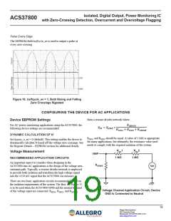
BYPASSING THE DYNAMIC FRAMING OF THE RMS
CALCULATION WINDOW
OCF
DIO_1
By default, the ACS37800 dynamically calculates the value of
N to be used in the RMS and power calculations based on the
zero crossings on the voltage channel. This functionality can be
disabled using the bypass_n_en field.
UVRMS
OVRMS
OCF_LAT
DIO_1 / CS
CS
DIO_1_Sel[0..1]
Comm_Sel
16
Allegro MicroSystems
955 Perimeter Road
Manchester, NH 03103-3353 U.S.A.
www.allegromicro.com

 ALLEGRO [ ALLEGRO MICROSYSTEMS ]