Isolated, Digital Output, Power Monitoring IC
with Zero-Crossing Detection, Overcurrent and Overvoltage Flagging
ACS37800
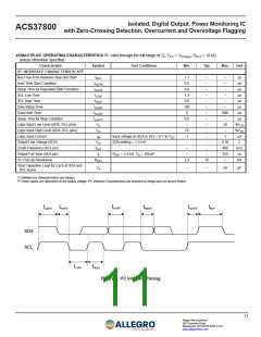
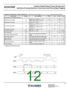
xKMATR-SPI OPERATING CHARACTERISTICS [1]: Valid through the full range of TA, VCC = VCC(typ), unless otherwise specified
Characteristic
Symbol
Test Conditions
Min.
Typ.
Max.
Unit
SPI INTERFACE CHARACTERISTICS
MOSI, SCLK, CS pins, VCC = 3.3 V
MOSI, SCLK, CS pins, VCC = 5 V
MOSI, SCLK, CS pins
2.8
4
–
–
–
3.63
5.5
V
V
V
Digital Input High Voltage
Digital Input Low Voltage
VIH
VIL
–
0.5
MISO pin, CL = 20 pF, TA = 25°C,
VCC(typ) = 3.3 V
2.8
4
3.3
5
3.8
5.5
V
V
SPI Output High Voltage
VOH
MISO pin, CL = 20 pF, TA = 25°C,
VCC(typ) = 5 V
SPI Output Low Voltage
SPI Clock Frequency
SPI Frame Rate
VOL
fSCLK
tSPI
MISO pin, CL = 20 pF, TA = 25°C
MISO pin, CL = 20 pF
–
0.3
–
0.5
10
V
0.1
5.8
MHz
kHz
–
588
Time from CS going low to SCLK falling
edge
Chip Select to First SCLK Edge
tCS
50
–
–
ns
Data Output Valid Time
MOSI Setup Time
MOSI Hold Time
tDAV
tSU
Data output valid after SCLK falling edge
Input setup time before SCLK rising edge
Input hold time after SCLK rising edge
–
40
–
–
–
–
ns
ns
ns
25
50
tHD
–
Hold SCLK high time before CS rising
edge
SCLK to CS Hold Time
tCHD
CL
5
–
–
–
–
ns
Load Capacitance
Loading on digital output (MISO) pin
20
pF
[1] Validated by characterization and design.
Figure 3: SPI Timing
12
Allegro MicroSystems
955 Perimeter Road
Manchester, NH 03103-3353 U.S.A.
www.allegromicro.com

 ALLEGRO [ ALLEGRO MICROSYSTEMS ]