ASAHI KASEI
[AK4387]
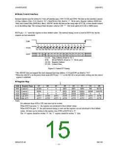
Register Definitions
Addr
Register Name
D7
ACKS
1
D6
0
D5
0
D4
DIF2
0
D3
DIF1
1
D2
DIF0
0
D1
PW
1
D0
RSTN
1
00H Control 1
default
0
0
RSTN: Internal timing reset control
0: Reset. All registers are not initialized.
1: Normal Operation
When MCLK frequency or DFS changes, the click noise can be reduced by RSTN bit.
PW: Power down control
0: Power down. All registers are not initialized.
1: Normal Operation
DIF2-0: Audio data interface formats (see Table 7)
Initial: “010”, Mode 2
ACKS: Master Clock Frequency Auto Setting Mode Enable
0: Disable, Manual Setting Mode
1: Enable, Auto Setting Mode
Master clock frequency is detected automatically at ACKS bit “1”. In this case, the setting of DFS1-0
are ignored. When this bit is “0”, DFS1-0 set the sampling speed mode.
Addr
Register Name
D7
DZFE
0
D6
1
D5
0
D4
DFS1
0
D3
DFS0
0
D2
DEM1
0
D1
DEM0
1
D0
SMUTE
0
01H Control 2
default
0
0
SMUTE: Soft Mute Enable
0: Normal operation
1: DAC outputs soft-muted
DEM1-0: De-emphasis Response (see Table 8)
Initial: “01”, OFF
DFS1-0: Sampling speed control
00: Normal speed
01: Double speed
10: Quad speed
When changing between Normal/Double Speed Mode and Quad Speed Mode, some click noise
occurs.
DZFE: Data Zero Detect Enable
0: Disable
1: Enable
Zero detect function can be disabled by DZFE bit “0”. In this case, the DZF pins of both channels are
always “L”.
MS0429-E-00
2005/09
- 16 -

 AKM [ ASAHI KASEI MICROSYSTEMS ]