ASAHI KASEI
[AK4387]
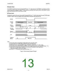
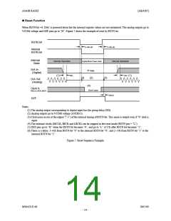
Reset Function
When RSTN bit =0, DAC is powered down but the internal register values are not initialized. The analog outputs go to
VCOM voltage and DZF pins go to “H”. Figure 7 shows the example of reset by RSTN bit.
RSTN bit
3~4/fs (6)
2~3/fs (6)
Internal
RSTN bit
Internal
State
Digital Block Power-down
“0” data
Normal Operation
Normal Operation
D/A In
(Digital)
GD
GD
(1)
(1)
(3)
(2)
(4)
(3)
D/A Out
(Analog)
Clock In
MCLK,LRCK,BICK
Don’t care
2/fs(5)
DZF
Notes:
(1) The analog output corresponding to digital input has the group delay (GD).
(2) Analog outputs go to VCOM voltage (AVDD/2).
(3) Click noise occurs at the edges(“ ”) of the internal timing of RSTN bit. This noise is output even if “0” data is
↑ ↓
input.
(4) The external clocks (MCLK, BICK and LRCK) can be stopped in the reset mode (RSTN pin = “L”).
(5) DZF pins go to “H” when the RSTN bit becomes “0”, and go to “L” at 2/fs after RSTN bit becomes “1”.
(6) There is a delay, 3~4/fs from RSTN bit “0” to the internal RSTN bit “0”, and 2~3/fs from RSTN bit “1” to the
internal RSTN bit “1”.
Figure 7. Reset Sequence Example
MS0429-E-00
2005/09
- 14 -

 AKM [ ASAHI KASEI MICROSYSTEMS ]