ASAHI KASEI
[AK4387]
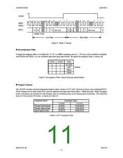
Mode Control Interface
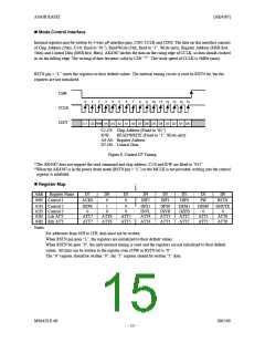
Internal registers may be written by 3-wire µP interface pins, CSN, CCLK and CDTI. The data on this interface consists
of Chip Address (2bits, C1/0; fixed to “01”), Read/Write (1bit; fixed to “1”, Write only), Register Address (MSB first,
5bits) and Control Data (MSB first, 8bits). AK4387 latches the data on the rising edge of CCLK, so data should clocked
in on the falling edge. The writing of data becomes valid by CSN “ ”. The clock speed of CCLK is 5MHz (max).
↑
RSTN pin = “L” resets the registers to their default values. The internal timing circuit is reset by RSTN bit, but the
registers are not initialized.
CSN
0
1
2
3
4
5
6
7
8
9
10 11 12 13 14 15
CCLK
CDTI
C1 C0 R/W A4 A3 A2 A1 A0 D7 D6 D5 D4 D3 D2 D1 D0
C1-C0: Chip Address (Fixed to “01”)
R/W:
READ/WRITE (Fixed to “1”, Write only)
A4-A0: Register Address
D7-D0: Control Data
Figure 8. Control I/F Timing
*The AK4387 does not support the read command and chip address. C1/0 and R/W are fixed to “011”
*When the AK4387 is in the power down mode (RSTN pin = “L”) or the MCLK is not provided, writing into the control
register is inhibited.
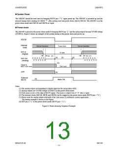
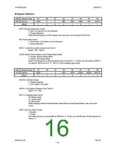
Register Map
Addr
Register Name
D7
D6
0
D5
0
D4
D3
D2
D1
D0
00H Control 1
ACKS
DIF2
DIF1
DIF0
PW
RSTN
01H Control 2
02H Control 3
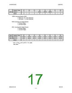
03H Lch ATT
04H Rch ATT
DZFE
0
ATT7
ATT7
1
0
0
0
DFS1
INVL
ATT4
ATT4
DFS0
INVR
ATT3
ATT3
DEM1
DZFB
ATT2
ATT2
DEM0
0
ATT1
ATT1
SMUTE
0
ATT0
ATT0
ATT6
ATT6
ATT5
ATT5
Notes:
For addresses from 05H to 1FH, data must not be written.
When RSTN pin goes “L”, the registers are initialized to their default values.
When RSTN bit goes “0”, the only internal timing is reset and the registers are not initialized to their default
values. All data can be written to the register even if PW or RSTN bit is “0”.
The “0” register should be written “0”, the “1” register should be written “1” data.
MS0429-E-00
2005/09
- 15 -

 AKM [ ASAHI KASEI MICROSYSTEMS ]