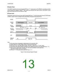
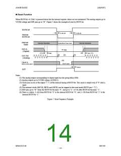
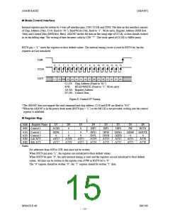
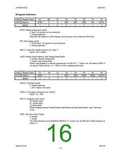
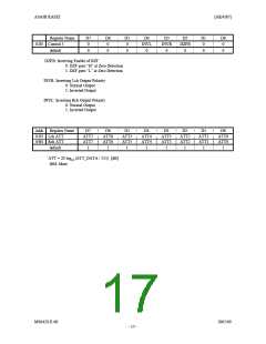
ASAHI KASEI
[AK4387]
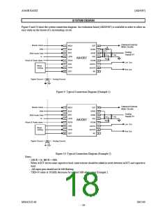
SYSTEM DESIGN
Figure 9 and 10 show the system connection diagram. An evaluation board (AKD4387) is available in order to allow an
easy study on the layout of a surrounding circuit.
Optional External
Mute Circuits
Master Clock
64fs
MCLK
BICK
SDTI
DZF
1
2
3
4
5
6
7
8
16
10
0.1u
0.1u
10u
DVDD 15
AVDD 14
Analog
Supply 5V
24bit Audio Data
fs
+
10u
LRCK
RSTN
CSN
VSS
13
AK4387
+
Reset & Power down
VCOM 12
AOUTL 11
Lch Out
Rch Out
Mode
Setting
CCLK
AOUTR
NC
10
9
CDTI
Digital Ground
Analog Ground
Figure 9. Typical Connection Diagram (Example 1)
Optional External
Mute Circuits
Master Clock
64fs
MCLK
BICK
SDTI
DZF
1
2
3
4
5
6
7
8
16
DVDD 15
AVDD 14
Analog
Supply 5V
24bit Audio Data
fs
+
10u
0.1u
10u
LRCK
RSTN
CSN
VSS
13
AK4387
+
Reset & Power down
VCOM 12
AOUTL 11
Lch Out
Rch Out
Mode
Setting
CCLK
AOUTR
NC
10
9
CDTI
Digital Ground
Analog Ground
Figure 10. Typical Connection Diagram (Example 2)
Notes:
- LRCK = fs, BICK = 64fs.
- When AOUT drives some capacitive load, some resistor should be added in series between AOUT and capacitive
load.
- All input pins should not be left floating.
- THD+N value at 192kHz decreases by around 3dB when using Example 2.
MS0429-E-00
2005/09
- 18 -

 AKM [ ASAHI KASEI MICROSYSTEMS ]