[AK4372]
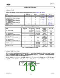
■ PLL Slave Mode (PMPLL bit = “1”, M/S bit = “0”)
A reference clock of PLL is selected among the input clocks to the MCKI, BICK or LRCK pin. The required clock to the
AK4372 is generated by an internal PLL circuit. Input frequency is selected by PLL4-0 bits (Table 4).
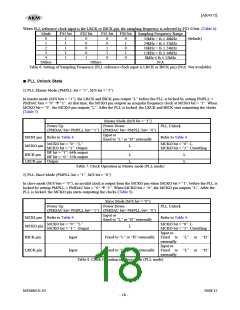
a) PLL reference clock: MCKI pin
BICK and LRCK inputs should be synchronized with MCKO output. The phase between MCKO and LRCK dose not
matter. The MCKO pin outputs the frequency selected by PS1-0 bits (Table 9) and the output is enabled by MCKO bit.
Sampling frequency can be selected by FS3-0 bits (Table 5).
The external clocks (MCKI, BICK and LRCK) should always be present whenever the DAC is in operation (PMDAC bit
= “1”). If these clocks are not provided, the AK4372 may draw excess current and will not possible to operate properly
because it utilizes dynamic refreshed logic internally. If the external clocks are not present, the DAC should be in the
power-down mode (PMDAC bits = “0”).
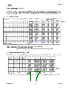
27MHz,26MHz,19.8MHz,19.68MHz,
19.2MHz,15.36MHz,14.4MHz,13MHz,
12MHz,11.2896MHz
AK4372
DSP or μP
MCKI
256fs/128fs/64fs/32fs
MCLK
BCLK
LRCK
MCKO
BICK
32fs ~ 64fs
1fs
LRCK
SDTO
SDATA
Figure 12. PLL Slave Mode (PLL Reference Clock: MCKI pin)
b) PLL reference clock: BICK pin
Sampling frequency corresponds to 8kHz to 48kHz by changing FS3-0 bits (Table 6).
AK4372
DSP or μP
MCKI
MCKO
32fs or 64fs
BCLK
LRCK
BICK
1fs
LRCK
SDTO
SDATA
Figure 13. PLL Slave Mode (PLL Reference Clock: BICK pin)
MS0684-E-02
2008/12
- 20 -

 AKM [ ASAHI KASEI MICROSYSTEMS ]