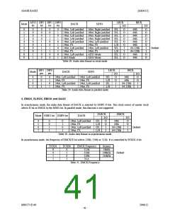
ASAHI KASEI
[AK4115]
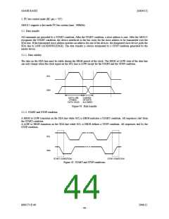
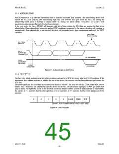
2-1-3. ACKNOWLEDGE
ACKNOWLEDGE is a software convention used to indicate successful data transfers. The transmitting device will
release the SDA line (HIGH) after transmitting eight bits. The receiver must pull down the SDA line during the
acknowledge clock pulse so that that it remains stable “L” during “H” period of this clock pulse. The AK4115 will
generates an acknowledge after each byte has been received.
In the read mode, the slave, AK4115 will transmit eight bits of data, release the SDA line and monitor the line for an
acknowledge. If an acknowledge is detected and no STOP condition is generated by the master, the slave will continue to
transmit data. If an acknowledge is not detected, the slave will terminate further data transmissions and await the STOP
condition.
Clock pulse
for acknowledge
SCL FROM
MASTER
1
8
9
DATA
OUTPUT BY
TRANSMITTER
not acknowledge
acknowledge
DATA
OUTPUT BY
RECEIVER
START
CONDITION
Figure 43. Acknowledge on the I2C-bus
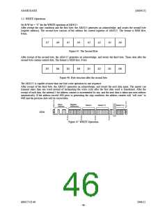
2-1-4. FIRST BYTE
The first byte, which includes seven bits of slave address and one bit of R/W bit, is sent after the START condition. If the
transmitted slave address matches an address for one of the device, the receiver who has been addressed pulls down the
SDA line.
The most significant five bits of the slave address are fixed as “00100”. The next two bits are CAD1 and CAD0 (device
address bits). These two bits identify the specific device on the bus. The hard-wired input pins (CAD1 pin and CAD0
pin) set them. The eighth bit (LSB) of the first byte (R/W bit) defines whether a write or read condition is requested by
the master. A “1” indicates that the read operation is to be executed. A “0” indicates that the write operation is to be
executed.
0
0
1
0
0
CAD1 CAD0
R/W
(Those CAD1/0 should match with CAD1/0 pins.)
Figure 44. The First Byte
MS0573-E-00
2006/12
- 45 -

 AKM [ ASAHI KASEI MICROSYSTEMS ]