ASAHI KASEI
[AK4115]
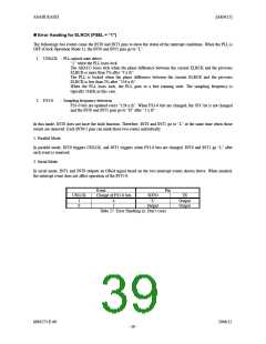
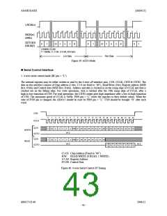
LRCK(o)
27
28
0
1
2
24
25
26
31
0
1
2
24
25
26 27
31
0
1
28
BICK(o)
(64fs)
SDTO(0)
DAUX(I)
0
1
2
23
V
U
0
1
2
23
V
U
C
B
0
1
C
B
23:MSB, 0:LSB
V: Validity, C: C-bit, U:U-bit, B:B sync
Lch Data
Rch Data
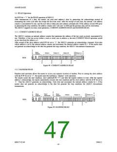
Figure 39. AES3 Mode
Serial Control Interface
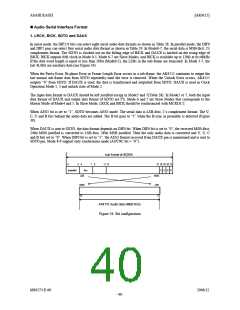
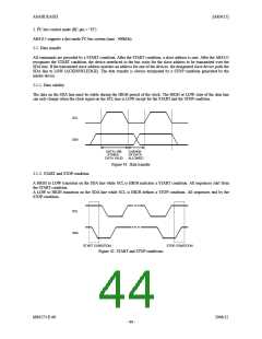
1. 4-wire serial control mode (IIC pin = “L”)
The internal registers may be either written or read by the 4-wire P interface pins: CSN, CCLK, CDTI & CDTO. The
µ
data on this interface consists of Chip address (2-bits, C1-0 are fixed to “00”), Read/Write (1bit), Register address (MSB
first, 8-bits) and Control data (MSB first, 8-bits). Address and data is clocked in on the rising edge of CCLK and data is
clocked out on the falling edge. For write operations, data is latched after the 24th rising edge of CCLK, after a
high-to-low transition of CSN. For read operations, the CDTO output goes high impedance after a low-to-high transition
of CSN. The maximum speed of CCLK is 5MHz. PDN pin = “L” resets the registers to their default values. When the
state of P/SN pin is changed, the AK4115 should be reset by PDN pin = “L”. CSN should be brought “H” after each
word.
CSN
8
9
10 11 12 13 14 15
16 17 18 19 20 21 22 23
0
1
2
0
0
3
0
0
4
0
0
5
0
6
0
7
CCLK
CDTI
CDTO
CDTI
A7 A6 A5 A4 A3 A2 A1 A0
D7 D6 D5 D4 D3 D2 D1 D0
C1 C0
C1 C0
R/W
WRITE
READ
Hi-Z
0
0
R/W A7 A6 A5 A4 A3 A2 A1 A0 D7 D6 D5 D4 D3 D2 D1 D0
D7 D6 D5 D4 D3 D2 D1 D0
Hi-Z
Hi-Z
CDTO
C1-C0: Chip Address (Fixed to “00”)
R/W: READ/WRITE (0:READ, 1:WRITE)
A7-A0: Register Address
D7-D0: Control Data
Figure 40. 4-wire Serial Control I/F Timing
MS0573-E-00
2006/12
- 43 -

 AKM [ ASAHI KASEI MICROSYSTEMS ]