Ambassador T8100A, T8102, and T8105
H.100/H.110 Interfaces and Time-Slot Interchangers
Advance Data Sheet
November 1999
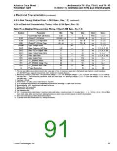
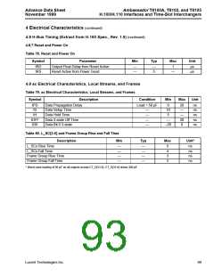
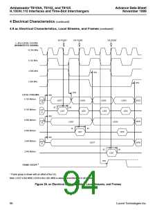
4 Electrical Characteristics (continued)
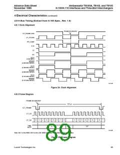
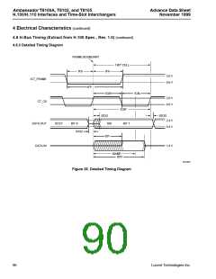
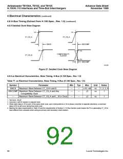
4.8 H-Bus Timing (Extract from H.100 Spec., Rev. 1.0) (continued)
4.8.4 ac Electrical Characteristics, Timing, H-Bus (H.100 Spec., Rev. 1.0)
Table 76. ac Electrical Characteristics, Timing, H-Bus (H.100 Spec., Rev. 1.0)
Symbol
Parameter
Min
Typ
Max
Unit
Notes
—
tC8P
tC8H
tC8L
tSAMP
tDOZ
tZDO
tDOD
tDV
Clock Edge Rate (all clocks)
Clock CT_C8 Period
Clock CT_C8 High Time
Clock CT_C8 Low Time
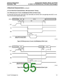
Data Sample Point
0.25
—
—
—
—
90
—
—
—
—
—
122
—
—
—
2
V/ns
ns
ns
ns
ns
ns
ns
ns
ns
ns
ns
ns
ns
ns
1, 2, 4
2, 4, 5
122.066 – Φ
122.074 + Φ
49 – Φ
49 – Φ
—
73 + Φ
73 + Φ
—
2, 4, 6
2, 4, 6
2, 4, 9
Data Output to HiZ Time
Data HiZ to Output Time
Data Output Delay Time
Data Valid Time
–20
0
0
2, 3, 4, 7, 11
2, 3, 4, 7, 11
2, 3, 4, 7
2, 3, 4, 8, 10
2, 4
22
0
22
0
69
tDIV
tFP
Data Invalid Time
102
90
112
180
90
/CT_FRAME Width
2, 4
tFS
/CT_FRAME Setup Time
/CT_FRAME Hold Time
Phase Correction
45
2, 4
tFH
45
90
2, 4
Φ
0
10
12
1. The rise and fall times are determined by the edge rate in V/ns. A maximum edge rate is the fastest rate at which a clock transitions.
CT_NETREF has a separate requirement. (See Section 2.5 Clocking Section.)
2. Measuring conditions, data lines: VTH (threshold voltage) = 1.4 V, VHI (test high voltage) = 2.4 V, VLO (test low voltage) = 0.4 V, input sig-
nal edge rate = 1 V/ns measuring conditions, clock and frame lines: Vt+ (test high voltage) = 2.0 V, Vt– (test low voltage) = 0.6 V, input sig-
nal edge rate = 1 V/ns.
3. Test load—200 pF.
4. When RESET is active, every output driver is 3-stated.
5. tC8P minimum and maximum are under free-run conditions assuming ±32 ppm clock accuracy.
6. Noncumulative, tC8P requirements still need to be met.
7. Measured at the transmitter.
8. Measured at the receiver.
9. For reference only.
10. tDV = maximum clock cable delay + maximum data cable delay + maximum data HiZ to output time = 12 ns + 35 ns + 22 ns = 69 ns. Maxi-
mum clock cable delay and maximum data cable delay are worst-case numbers based on electrical simulation.
11. tDOZ and tZDO apply at every time-slot boundary.
12. F (phase correction) results from PLL timing corrections.
Lucent Technologies Inc.
87

 AGERE [ AGERE SYSTEMS ]