Ambassador T8100A, T8102, and T8105
H.100/H.110 Interfaces and Time-Slot Interchangers
Advance Data Sheet
November 1999
4 Electrical Characteristics (continued)
4.8 H-Bus Timing (Extract from H.100 Spec., Rev. 1.0) (continued)
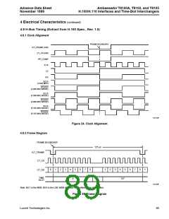
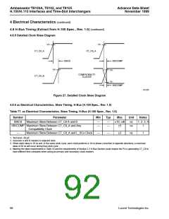
4.8.5 Detailed Clock Skew Diagram
Vt+
Vt+
CT_C8_A
CT_C8_A
tSKC8
tSKCOMP
Vt+
Vt+
COMPATIBILITY
CLOCKS
CT_C8_B
Vt–
tSKCOMP
5-6122F
Figure 27. Detailed Clock Skew Diagram
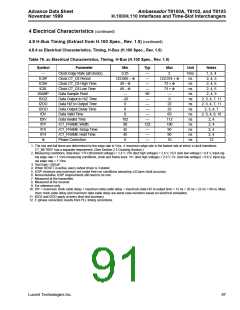
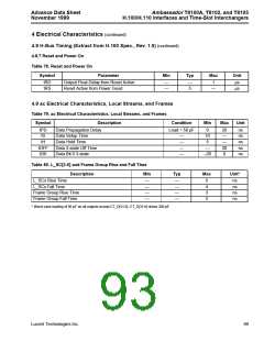
4.8.6 ac Electrical Characteristics, Skew Timing, H-Bus (H.100 Spec., Rev. 1.0)
Table 77. ac Electrical Characteristics, Skew Timing, H-Bus (H.100 Spec., Rev. 1.0)
Symbol
Parameter
Min
Typ
Max
Unit
Notes
tSKC8
Maximum Skew Between CT_C8 A and B
—
—
—
—
±10, ±Φ
ns
ns
1, 2, 3, 4
1
tSKCOMP Maximum Skew Between CT_C8_A and Any
Compatibility Clock
±5
—
Maximum Skew Between CT_C8_A and L_SCx Clock
—
—
±2
ns
1
1. Test load—50 pF.
2. Assumes A and B masters in adjacent slots.
3. When static skew is 10 ns and, in the same clock cycle, each clock performs a 10 ns phase correction in opposite directions, a maximum
skew of 30 ns will occur during that clock cycle.
4. Meeting the skew requirements in Table 10 and the requirements of Section 2.3 H-Bus Section could require the PLLs generating CT_C8 to
have different time constants when acting as primary and secondary clock masters.
88
Lucent Technologies Inc.

 AGERE [ AGERE SYSTEMS ]