Ambassador T8100A, T8102, and T8105
H.100/H.110 Interfaces and Time-Slot Interchangers
Advance Data Sheet
November 1999
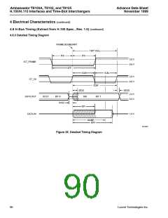
4 Electrical Characteristics
4.1 Absolute Maximum Ratings
Stresses in excess of the absolute maximum ratings can cause permanent damage to the device. These are abso-
lute stress ratings only. Functional operation of the device is not implied at these or any other conditions in excess
of those given in the operational sections of this data sheet. Exposure to absolute maximum ratings for extended
periods can adversely affect device reliability.
Description
Symbol
Min
Max
Unit
Supply Voltage
VDD
—
—
VSS
3.6
VDD
V
V
V
XTALIN and XTALOUT Pins
Voltage Applied to I/O Pins
—
VSS – 0.5
VDD + 3.4
Operating Temperature:
208-pin SQFP
217-ball BGA
—
—
0
−40
70
85
°C
°C
Storage Temperature
Tstg
–55
125
°C
4.2 Handling Precautions
Although protection circuitry has been designed into this device, proper precautions should be taken to avoid expo-
sure to electrostatic discharge (ESD) during handling and mounting. Lucent employs a human-body model (HBM)
and a charged-device model (CDM) for ESD-susceptibility testing and protection design evaluation. ESD voltage
thresholds are dependent on the circuit parameters used to define the model. No industry-wide standard has been
adopted for CDM. However, a standard HBM (resistance = 1500 Ω, capacitance = 100 pF) is widely used and,
therefore, can be used for comparison purposes:
HBM ESD Threshold Voltage
Device
Rating
T8100A, T8102, T8105
2500 V
82
Lucent Technologies Inc.

 AGERE [ AGERE SYSTEMS ]