Ambassador T8100A, T8102, and T8105
H.100/H.110 Interfaces and Time-Slot Interchangers
Advance Data Sheet
November 1999
2 Architecture and Functional Description (continued)
2.9 Testing and Diagnostics (continued)
2.9.2 Diagnostics (continued)
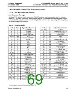
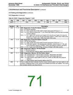
Table 63. DIAG1: Diagnostics Register 1, 0x30
Reg
R/W
Bit 7
Bit 6
Bit 5
Bit 4
Bit 3
Bit 2
Bit 1
Bit 0
DIAG1
—
DFA
DFB
DMF
DMP
DMD
Symbol
Bit
Description
DFA
7—6
DFA: Diagnostics, Frame Pin Selects, Group A
DFA = 00, Normal operation.
DFA = 01, State counter bits [10:0] routed to frame group pins [10:0], pin 11 = L.
DFA = 10, Even CAM hit routed to pin 11, pin 10 has odd CAM hit, pins [9:0] have local data
memory address.
DFA = 11, Pin 11 gets CUE error bit, pin 10 gets CUO error bit, pin 9 gets CUL error bit,
pin 8 gets COE error bit, pins [5:0] get page pointers—8 MHz read, 8 MHz write,
4 MHz read, 4 MHz write, 2 MHz read, and 2 MHz write.
DFB
5—4
DFB: Diagnostics, Frame Pin Selects, Group B
DFB = 00, Normal operation.
DFB = 01, State counter bits [10:0] routed to frame group pins [10:0], pin 11 = L.
DFB = 10, CAM state register [1:0] indicating four substates, routed to pins [11:10], and
local connection memory (T8100A, T8105 only) address routed to pins [9:0].
DFB = 11, Pin 11 gets local CAM hit flag, and pins [10:0] get CAM state counter.
DMF
DMP
3
DMF: Diagnostics, Memory, Fill Test Enable
DMF = 0, Normal operation.
DMF = 1, Fill all memories with the pattern selected by DMP.
2—1
DMP: Diagnostics, Memory, Fill Test Pattern Select
DMP = 00, Checkerboard 0—even locations get 0x55, odd locations get 0xAA.
DMP = 01, Checkerboard 1—even locations get 0xAA, odd locations get 0x55.
DMP = 10, Data locations equal address bits [7:0]. (CAMs are filled with their physical
address.)
DMP = 11, Data locations equal inverted address bits [7:0].
DMD
0
This is a status bit which indicates that the chosen memory pattern has been written to all
locations. Additional writes to the memory are disabled and reads are enabled. This condi-
tion remains until the user clears this bit.
Lucent Technologies Inc.
67

 AGERE [ AGERE SYSTEMS ]