Ambassador T8100A, T8102, and T8105
H.100/H.110 Interfaces and Time-Slot Interchangers
Advance Data Sheet
November 1999
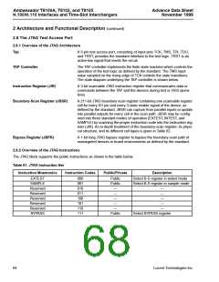
2 Architecture and Functional Description (continued)
2.7 Error Registers (continued)
The CKW register works in conjunction with the two registers above and with the clock circuitry. It is used to enable
the watchdogs for the clock lines. CKW uses the same mapping as CLKERR1 and CLKERR2, so, for example, a
high in bit 7 will enable the watchdogs for CT_C8A and /CT_FRAMEA. CKW functions as a masking register for
CLKERR1 and CLKERR2. If the appropriate bit is not set, then a failing clock will not be reported. CLKERR3 bit 0
functions as the mask bit for CT_NETREF2 errors.
The SYSERR and CLKERR1 bits, when set, will remain set until they are reset. To reset and clear the two regis-
ters, set the correpsonding bit(s) in the MCR (see Section 2.1 Register/Memory Maps). When clearing the MCR
registers, it takes between one and two state machine clock cycles (15.25 ns to 30.5 ns) from the trailing edge of
WRn strobe to assertion of the internal CER/SER strobes. These internal strobes immediately (asynchronously)
reset their respective registers.
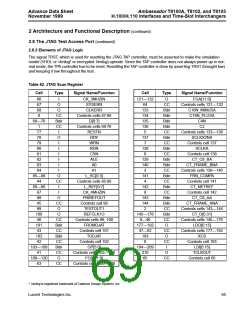
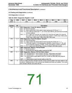
Table 59. CLKERR3: Error Indicator and Current Status, 0x2C
Reg
R/W
Bit 7
Bit 6
Bit 5
Bit 4
Bit 3
Bit 2
Bit 1
Bit 0
CLKERR3
R/W
RES
N2E
N1E
RES
N2N
Symbol
RES
Bit
7—6 Reserved bit position. Read only.
Description
N2E
5
Read only.
N2E => Reports failures on CT_NETREF2.
N1E
4
Read only.
N1E => Reports failures on CT_NETREF1.
RES
N2N
3—1 Reserved bit position. Read/write.
0
Read/write.
N2N = 0, Disable error reporting on NETREF2.
N2N = 1, Enable error reporting on NETREF2.
Note: Bits [7:4] are read only, bits [3:0] are read/write.
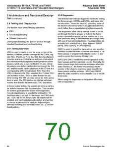
Table 60. SYSERR: System Error Register, 0x2A
Reg
R/W
Bit 7
Bit 6
Bit 5
Bit 4
Bit 3
Bit 2
Bit 1
Bit 0
SYSERR
—
CUE
CUO
CUL
COE
COO
COL
RES
FBE
Symbol
CUE
CUO
CUL
Bit
7
Description
CUE => Even CAM underflow, set by an unmatched comparison.
CUO => Odd CAM underflow, set by an unmatched comparison.
CUL => Local CAM underflow, set by an unmatched comparison.
COE => Even CAM overflow, set by a write to a full CAM.
COO => Odd CAM overflow, set by a write to a full CAM.
COL => Local CAM overflow, set by a write to a full CAM.
RES => Reserved bit position.
6
5
COE
COO
COL
4
3
2
RES
1
FBE
0
FBE => Fallback enabled, status which indicates that a clock error has occurred and fall-
back operations are in effect*.
* This error bit is selective. It will only flag an error if the clocks that fail correspond to the selected clock mode. For example, if MVIP mode is
selected (in register CKM), the proper fallback mode has been set (in register CKS), and the MVIP clocks are not masked (register CKW,
above), then FBE will go high when a failure is detected on /FR_COMPn, C2, or /C4. Thus, unmasked, failing non-MVIP clocks will be flagged
in the CLKERR1 and CLKERR2 registers but will not set the FBE flag in SYSERR.
Lucent Technologies Inc.
63

 AGERE [ AGERE SYSTEMS ]