Ambassador T8100A, T8102, and T8105
H.100/H.110 Interfaces and Time-Slot Interchangers
Advance Data Sheet
November 1999
2 Architecture and Functional Description (continued)
2.5 Clocking Section (continued)
2.5.8 Clock Control Register Definitions (continued)
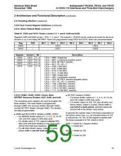
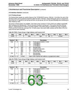
2.5.8.2 CKMD, CKND, CKRD: Clocks, Main, NETREF, Resource Dividers, 0x07, 0x08, and 0x09 (continued)
The CON register controls various features of the device. It has a bit for enabling/disabling the use of the GPD reg-
ister and a bit for selecting NETREF_1 or NETREF_2. It also has 3 bits for using the L_REF pairing feature. The
last 2 bits are programmed when using the minimum and constant delay settings for data transfers. The description
and use of the bit(s) for a particular feature is described in the section which pertains to the feature.
Table 52. CON Register 0x0E
Reg
R/W
Bit 7
Bit 6
Bit 5
Bit 4
Bit 3
Bit 2
Bit 1
Bit 0
CON
—
RES
GPDENB NETSEL LREFENB LREFIFS LREFIBC
CED
GFME
Symbol
Bit
Description
Reserved
GPDENB
7
6
Reserved.
0: Disables the GPD register.
1: Enables the GPD register.
NETSEL
LREFENB
LREFIFS
LREFIBC
CED
5
4
3
2
1
0
0: Select NETREF_1.
1: Select NETREF_2.
0: LREF’s are 8 unsynchronized inputs.
1: LREF’s are 4 pairs of synchronized inputs.
0: LREF frame strobe is not inverted.
1: LREF frame strobe is inverted.
0: LREF bit clock is not inverted.
1: LREF bit clock is inverted.
0: Individual FME bits are used for all transfers.
1: Value of GFME (CON register bit 0) is used for all transfers.
0: Only reverse connections provide constant delay.
1: Only forward connections provide constant delay.
GFME
56
Lucent Technologies Inc.

 AGERE [ AGERE SYSTEMS ]