Ambassador T8100A, T8102, and T8105
H.100/H.110 Interfaces and Time-Slot Interchangers
Advance Data Sheet
November 1999
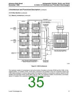
entry in the CAM on a location-by-location basis. (For
example, physical address 0xA7 in the CAM is coupled
with physical address 0xA7 of the register file.) The
CAMs will have only the comparand field for stream
and time-slot addresses, and the associated register
files will hold the data field, which is comprised of a tag
(an indirect pointer to the double-buffered data SRAM)
and some control bits. Using the associated SRAM
allows the operations to be pipelined so that the data
retrieval occurs while the CAMs are doing the next
comparison. The SRAM is double-buffered to permit
constant delay or minimum delay on a connection-by-
connection basis, as described in Section 2.2.1 Con-
stant Frame Delay and Minimum Delay Connections,
and as illustrated in Figure 5.
2 Architecture and Functional
Description (continued)
2.3 H-Bus Section
2.3.1 Memory Architecture
To access the H-bus, the devices use a new twist
on an existing approach to accessing large address
spaces: the data is stored in an independent double-
buffered SRAM which acts like the local data memory,
but the connection information for the H-bus is held in
three 512 location CAMs (T8102, T8105 only). Two
CAMs are used for two groups of 16 H-bus streams
each, and one CAM for all 16 local input/output pairs.
Each CAM compares 16 streams for read and write
and allows access time to the host microprocessor for
updates to the connections. Thus, each stream is
allotted three operations per 976 ns time slot, so there
are a maximum of 48 accesses per CAM per time
slot. The CAMs must operate at a rate of at least
20.34 ns/access*. The selected technology operates at
13 ns/access maximum, so an internal clock speed of
15.26 ns (65.536 MHz) is used.
* The H-bus presents a unique set of problems. A full nonblocking,
double-buffered switch of 5120 locations has significant barriers in
size and in control of memory access time. Further, the traffic
between the local bus and H-bus is generally limited to a small
number of time slots at any given moment (120 full duplex is typical,
although we are permitting 256 duplex or 512 (T8102, T8105 only)
simplex connections), but the requirement to access any time slot
out of the full range of 5120 locations remains. To solve this, content
addressable memories (CAM) are utilized. They provide access to
the full 5120 locations through an encoded width (13 bits), but
require a depth equal to the maximum number of connections
required (512 [T8102, T8105 only]).
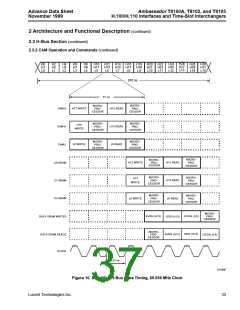
For the following discussions, the reader should refer to
Figure 9. The combined comparison plus retrieval
operations take two CAM cycles, leaving little time for
microprocessor updates. To circumvent this, a separate
SRAM (actually, a register file) is tied to each CAM.
Each entry of this register file is associated with an
30
Lucent Technologies Inc.

 AGERE [ AGERE SYSTEMS ]