Ambassador T8100A, T8102, and T8105
H.100/H.110 Interfaces and Time-Slot Interchangers
Advance Data Sheet
November 1999
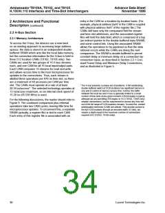
2 Architecture and Functional Description (continued)
2.2 Local Bus Section (continued)
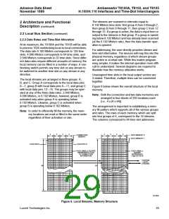
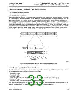
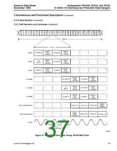
2.2.5 State Counter Operation
All operations are synchronized to the master state counter. The state counter is, in turn, synchronized to the inter-
nal frame signal and driven by an internal 65.536 MHz clock. In normal operation, the internal frame and clock are
synchronized to either the H-bus or trunks (see Section 2.5 Clocking Section for a more detailed explanation of
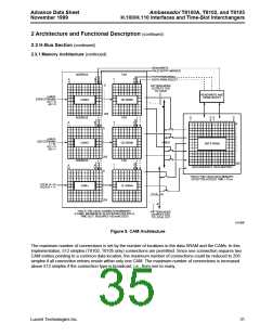
clocking options). The local memory states (T8100A, T8105 only) are illustrated in Figure 8. The state counter is a
modulo-8192 counter (7 bits for time slot, 4 bits for stream, 2 bits for state function) which can also be reset and
loaded with other values for diagnostic purposes (as described in Section 2.9 Testing and Diagnostics). The H-bus
memories are also referenced to this state counter so that the devices maintain synchronization with the H-bus to
ensure proper access to the bus as well as ensure synchronization between the H-bus and local memory struc-
tures. The H-bus memories are discussed in Section 2.3 H-Bus Section.
L13
L0
L1
L2
L3
L4
L5
L6
L7
L8
L9
L10 L11 L12
L14 L15
976 ns
61 ns
CONNECTION
MEMORY
H6 READ
MICROPROCESSOR
MICRO-
PRO-
CESSOR
MICRO-
DATA
SRAM
H6 WRITE
H6 READ
PRO-
CESSOR
CLOCK
15.25 ns
5-6107F
Figure 8. Simplified Local Memory State Timing, 65.536 MHz Clock
2.2.6 Software to Reset the Local Connection Memory
When the device is powered up, random connections may exist. To clear the upper 6 bits and, therefore, all control
bits, the following sequence of instructions should be followed:
1. Write AMR = 0x00.
2. Write LAR = 0x30.
3. Write IDR = 0x0C.
4. Monitor Diag-1, 0x30, bit 0. This bit is set when the operation is complete (steps 1 through 3).
5. Write LAR = 0x30.
6. Write IDR = 0x00. This brings the device out of diagnostics mode.
After executing the instructions, the contents of the local connection memory will contain its corresponding 10-bit
address. The upper 6 bits are cleared to zero. The lower 10 bits will have an address.
Lucent Technologies Inc.
29

 AGERE [ AGERE SYSTEMS ]