Ambassador T8100A, T8102, and T8105
H.100/H.110 Interfaces and Time-Slot Interchangers
Advance Data Sheet
November 1999
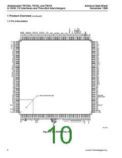
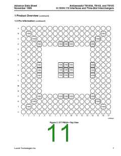
1 Product Overview (continued)
1.3 Pin Information (continued)
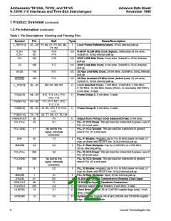
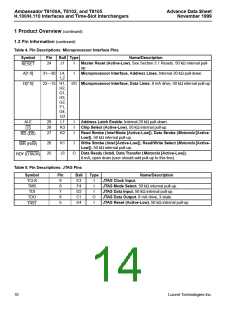
Table 4. Pin Descriptions: Microprocessor Interface Pins
Symbol
Pin
Ball Type
Name/Description
24
J1
I
Master Reset (Active-Low). See Section 3.1 Resets. 50 kΩ internal pull-
up.
RESET
A[1:0]
D[7:0]
31—30 L4,
L2
I
Microprocessor Interface, Address Lines. Internal 20 kΩ pull-down.
22—15 H1,
I/O Microprocessor Interface, Data Lines. 8 mA drive, 50 kΩ internal pull-up.
H2,
G1,
H3,
G2,
F1,
G4,
G3
ALE
29
28
27
L1
K3
K2
I
I
I
Address Latch Enable. Internal 20 kΩ pull-down.
Chip Select (Active-Low). 50 kΩ internal pull-up.
CS
Read Strobe (Intel Mode [Active-Low]), Data Strobe (Motorola [Active-
Low]). 50 kΩ internal pull-up.
RD (DS)
26
25
K1
J3
I
Write Strobe (Intel [Active-Low]), Read/Write Select (Motorola [Active-
Low]). 50 kΩ internal pull-up.
WR (R/W)
O
Data Ready (Intel), Data Transfer (Motorola [Active-Low]).
8 mA, open drain (user should add pull-up to this line).
RDY (DTACK)
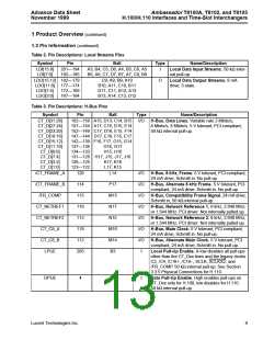
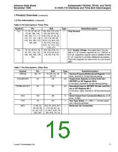
Table 5. Pin Descriptions: JTAG Pins
Symbol
TCLK
TMS
Pin
9
Ball
E3
F4
Type
Name/Description
I
I
JTAG Clock Input.
8
JTAG Mode Select. 50 kΩ internal pull-up.
JTAG Data Input. 50 kΩ internal pull-up.
JTAG Data Output. 8 mA drive, 3-state.
JTAG Reset (Active-Low). 50 kΩ internal pull-up.
TDI
7
D2
C1
E4
I
TDO
6
O
I
5
TRST
10
Lucent Technologies Inc.

 AGERE [ AGERE SYSTEMS ]