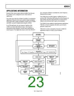
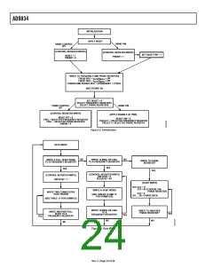
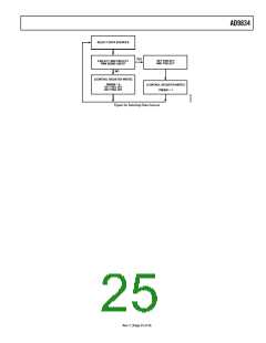
AD9834
INTERFACING TO MICROPROCESSORS
The AD9834 has a standard serial interface that allows the part
to interface directly with several microprocessors. The device
uses an external serial clock to write the data/control information
into the device. The serial clock can have a frequency of 40 MHz
maximum. The serial clock can be continuous, or it can idle high
or low between write operations. When data/control information is
being written to the AD9834, FSYNC is taken low and is held
low until the 16 bits of data are written into the AD9834. The
FSYNC signal frames the 16 bits of information being loaded
into the AD9834.
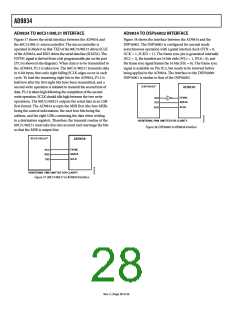
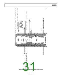
AD9834 TO 68HC11/68L11 INTERFACE
Figure 36 shows the serial interface between the AD9834 and
the 68HC11/68L11 microcontroller. The microcontroller is
configured as the master by setting Bit MSTR in the SPCR to 1,
providing a serial clock on SCK while the MOSI output drives
the serial data line SDATA. Because the microcontroller does
not have a dedicated frame sync pin, the FSYNC signal is
derived from a port line (PC7). The setup conditions for correct
operation of the interface are as follows:
• SCK idles high between write operations (CPOL = 0)
• Data is valid on the SCK falling edge (CPHA = 1)
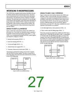
AD9834 TO ADSP-21xx INTERFACE
Figure 35 shows the serial interface between the AD9834 and
the ADSP-21xx. The ADSP-21xx should be set up to operate in
the SPORT transmit alternate framing mode (TFSW = 1). The
ADSP-21xx is programmed through the SPORT control register
and should be configured as follows:
When data is being transmitted to the AD9834, the FSYNC line is
taken low (PC7). Serial data from the 68HC11/68L11 is transmitted
in 8-bit bytes with only eight falling clock edges occurring in the
transmit cycle. Data is transmitted MSB first. To load data into
the AD9834, PC7 is held low after the first eight bits are transferred
and a second serial write operation is performed to the AD9834.
Only after the second eight bits have been transferred should
FSYNC be taken high again.
• Internal clock operation (ISCLK = 1)
• Active low framing (INVTFS = 1)
• 16-bit word length (SLEN = 15)
68HC11/68L111
AD98341
• Internal frame sync signal (ITFS = 1)
• Generate a frame sync for each write (TFSR = 1)
PC7
MOSI
SCK
FSYNC
SDATA
Transmission is initiated by writing a word to the Tx register
after the SPORT has been enabled. The data is clocked out on
each rising edge of the serial clock and clocked into the AD9834
on the SCLK falling edge.
SCLK
1
ADDITIONAL PINS OMITTED FOR CLARITY.
Figure 36. 68HC11/68L11 to AD9834 Interface
ADSP-21xx1
AD98341
FSYNC
SDATA
TFS
DT
SCLK
SCLK
1
ADDITIONAL PINS OMITTED FOR CLARITY.
Figure 35. ADSP-21xx to AD9834 Interface
Rev. C | Page 27 of 36

 ADI [ ADI ]