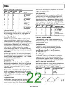
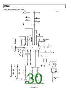
AD9834
GROUNDING AND LAYOUT
The printed circuit board (PCB) that houses the AD9834 should be
designed so that the analog and digital sections are separated
and confined to certain areas of the board. This facilitates the
use of ground planes that can easily be separated. A minimum
etch technique is generally best for ground planes because it
gives the best shielding. Digital and analog ground planes
should only be joined in one place. If the AD9834 is the only
device requiring an AGND-to-DGND connection, the ground
planes should be connected at the AGND and DGND pins of
the AD9834. If the AD9834 is in a system where multiple devices
require AGND-to-DGND connections, the connection should
be made at one point only, establishing a star ground point as
close as possible to the AD9834.
Good decoupling is important. The analog and digital supplies
to the AD9834 are independent and separately pinned out to
minimize coupling between analog and digital sections of the
device. All analog and digital supplies should be decoupled to
AGND and DGND, respectively, with 0.1 μF ceramic capacitors
in parallel with 10 μF tantalum capacitors. To achieve the best
performance from the decoupling capacitors, they should be
placed as close as possible to the device, ideally right up against
the device. In systems where a common supply is used to drive
both the AVDD and DVDD of the AD9834, it is recommended
that the system’s AVDD supply be used. This supply should have
the recommended analog supply decoupling between the
AVDD pins of the AD9834 and AGND, and the recommended
digital supply decoupling capacitors between the DVDD pins
and DGND.
Avoid running digital lines under the device because these
couple noise onto the die. The analog ground plane should be
allowed to run under the AD9834 to avoid noise coupling. The
power supply lines to the AD9834 should use as large a track as
possible to provide low impedance paths and reduce the effects
of glitches on the power supply line. Fast switching signals, such
as clocks, should be shielded with digital ground to avoid radiating
noise to other sections of the board. Avoid crossover of digital
and analog signals. Traces on opposite sides of the board should
run at right angles to each other to reduce the effects of feed-
through through the board. A microstrip technique is by far the
best, but it is not always possible with a double-sided board. In
this technique, the component side of the board is dedicated to
ground planes and signals are placed on the other side.
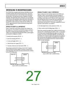
Proper operation of the comparator requires good layout strategy.
The strategy must minimize the parasitic capacitance between
VIN and the SIGN BIT OUT pin by adding isolation using a
ground plane. For example, in a multilayered board, the VIN
signal could be connected to the top layer, and the SIGN BIT OUT
could be connected to the bottom layer so that isolation is
provided by the power and ground planes between them.
Rev. C | Page 26 of 36

 ADI [ ADI ]