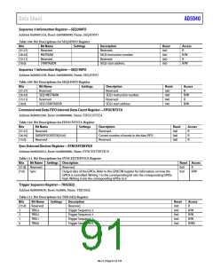
Data Sheet
AD5940
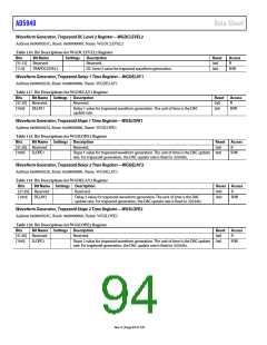
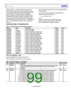
Waveform Generator, Sinusoid Frequency Control Word Register—WGFCW
Address 0x00002030, Reset: 0x00000000, Name: WGFCW
Table 121. Bit Descriptions for WGFCW Register
Bits
[31:24] Reserved
[30:0] SINEFCW
Bit Name Settings Description
Reset Access
Reserved.
0x0
0x0
R
R/W
Sinusoid generator frequency control word. These bits select the output frequency
of the sinusoid waveform. The output frequency (fOUT) = fACLK × (SINEFCW/230). To obtain
accurate DFT results and to avoid spectral leakage, fOUT/(DFT input data rate/N) must
be an integer, where N is input data number of DFT. Refer to the DFTNUM bit in the
DFTCON register (see Table 48). The DFT input data rate can be different due to
different input data sources. Refer to the DFTINSEL bit in the DFTCON register (see
Table 48).
Sinc3 is output as input data of DFT (the DFT input data rate = ADC output data
rate(1.6 MHz or 800 kHz)/SINC3_OSR)). Refer to the SINC3OSR bit in the
ADCFILTERCON register (see Table 42). For the sinc3 bypass, refer to the SINC3BYP bit in
the ADCFILTERCON register (see Table 42).
If the DFT input data rate = 800 kHz, the ADC output data rate must be set to 800 kHz.
Refer to the ADCSAMPLERATE bit in the ADCFILTERCON register = 1 (see Table 42). The
general formula is ADC_FS/SINC3_OSR/SINC2_OS. Refer to the SINC2OSR bit in the
ADCFILTERCON register (see Table 42).
For more information, see the High Performance ADC Circuit section.
Waveform Generator, Sinusoid Phase Offset Register—WGPHASE
Address 0x00002034, Reset: 0x00000000, Name: WGPHASE
Table 122. Bit Descriptions for WGPHASE Register
Bits
[31:20] Reserved
[19:0] SINEOFFSET
Bit Name
Settings
Description
Reserved.
Reset Access
0x0
0x0
R
R/W
Sinusoid phase offset. SINEOFFSET, Bits[19:0] = phase (degrees)/360 × 220. For
example, to obtain a 45° phase offset, SINEOFFSET, Bits[19:0] = 45/360 × 220. This
register must be set before setting the TYPESEL bit in the WGCON register and
the WAVEGENEN bit in the AFECON register.
Waveform Generator, Sinusoid Offset Register—WGOFFSET
Address 0x00002038, Reset: 0x00000000, Name: WGOFFSET
Table 123. Bit Descriptions for WGOFFSET Register
Bits
[31:12] Reserved
[11:0] SINEOFFSET
Bit Name
Settings Description
Reset Access
Reserved.
0x0
0x0
R
R/W
Sinusoid offset. This offset is added to the waveform generator output in sinusoid
mode. This value is a signed number represented in twos complement format. This
register must be set before setting the TYPESEL bit in the WGCON register and the
WAVEGENEN bit in the AFECON register.
Waveform Generator, Sinusoid Amplitude Register—WGAMPLITUDE
Address 0x0000203C, Reset: 0x00000000, Name: WGAMPLITUDE
Table 124. Bit Descriptions for WGAMPLITUDE Register
Bits
[31:11] Reserved
[10:0] SINEAMPLITUDE
Bit Name
Settings Description
Reset Access
Reserved.
0x0
0x0
R
R/W
Sinusoid amplitude, unsigned number. This amplitude scales the waveform
generator in sinusoid mode. The DAC output voltage is determined by this value,
as well as the ATTENEN bit and the INAMPGNMDE bit in the HSDACCON register.
This register must be set before setting the TYPESEL bit in the WGCON register
and the WAVEGENEN bit in the AFECON register.
Rev. 0 | Page 95 of 130

 ADI [ ADI ]