Data Sheet
AD5940
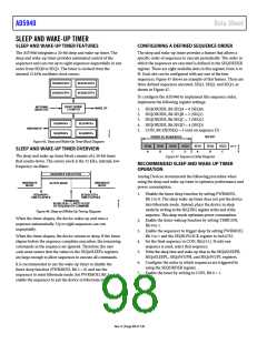
When CON, Bit 0 = 1, the timer loads the values from the
SEQxWUPH and SEQxWUPL registers and begins counting
down. When the timer reaches zero, the device wakes up and
executes sequences in the order specified in SEQORDER,
Bits[1:0]. The timer loads the values from the SEQxSLEEPH
and SEQxSLEEPL registers and begins counting down again
when the sequencer is running. When the timer elapses, the
AD5940 returns to sleep if TMRCON, Bit 0 = 1. If PWRMOD,
Bit 3 = 1, the AD5940 returns to sleep at the end of the last
sequence.
The maximum hibernate time is 32 sec when using the internal
32 kHz oscillator.
To calculate the code for SEQxWUPx and SEQxSLEEPx
registers, use the following equation:
Code = ClkFreq × Time
where:
Code is the code value for the SEQxWUPx register.
ClkFreq is frequency of the internal oscillator in Hz.
Time is required timeout duration in seconds.
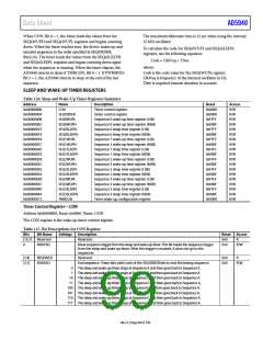
SLEEP AND WAKE-UP TIMER REGISTERS
Table 126. Sleep and Wake-Up Timer Registers Summary
Address
Name
CON
Description
Timer control register
Order control register
Reset
Access
R/W
R/W
R/W
R/W
R/W
R/W
R/W
R/W
R/W
R/W
R/W
R/W
R/W
R/W
R/W
R/W
R/W
R/W
R/W
0x00000800
0x00000804
0x00000808
0x0000080C
0x00000810
0x00000814
0x00000818
0x0000081C
0x00000820
0x00000824
0x00000828
0x0000082C
0x00000830
0x00000834
0x00000838
0x0000083C
0x00000840
0x00000844
0x00000A1C
0x0000
0x0000
0xFFFF
0x000F
0xFFFF
0x000F
0xFFFF
0x000F
0xFFFF
0x000F
0xFFFF
0x000F
0xFFFF
0x000F
0xFFFF
0x000F
0xFFFF
0x000F
0x0000
SEQORDER
SEQ0WUPL
SEQ0WUPH
SEQ0SLEEPL
SEQ0SLEEPH
SEQ1WUPL
SEQ1WUPH
SEQ1SLEEPL
SEQ1SLEEPH
SEQ2WUPL
SEQ2WUPH
SEQ2SLEEPL
SEQ2SLEEPH
SEQ3WUPL
SEQ3WUPH
SEQ3SLEEPL
SEQ3SLEEPH
TMRCON
Sequence 0 wake-up time register (LSB)
Sequence 0 wake-up time register (MSB)
Sequence 0 sleep time register (LSB)
Sequence 0 sleep time register (MSB)
Sequence 1 wake-up time register (LSB)
Sequence 1 wake-up time register (MSB)
Sequence 1 sleep time register (LSB)
Sequence 1 sleep time register (MSB)
Sequence 2 wake-up time register (LSB)
Sequence 2 wake-up time register (MSB)
Sequence 2 sleep time register (LSB))
Sequence 2 sleep time register (MSB)
Sequence 3 wake-up time register (LSB)
Sequence 3 wake-up time register (MSB)
Sequence 3 sleep time register (LSB)
Sequence 3 sleep time register (MSB)
Timer wake-up configuration register
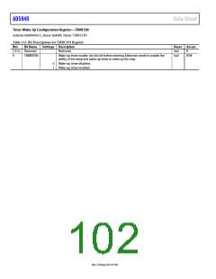
Timer Control Register—CON
Address 0x00000800, Reset: 0x0000, Name: CON
The CON register is the wake-up timer control register.
Table 127. Bit Descriptions for CON Register
Bits
Bit Name
Settings
Description
Reset Access
[15:7] Reserved
Reserved.
0x0
0x0
R
6
MSKTRG
Mask sequence trigger from the sleep and wake-up timer. This bit masks the sequence trigger
from the sleep and wake-up timer. After the trigger is masked, it does not go to the
sequencer.
R/W
[5:4]
[3:1]
RESERVED
ENDSEQ
Reserved.
0x0
0x0
R
End sequence. These bits select one of the SEQORDER bits to end the timing sequence.
The sleep and wake-up timer stops at Sequence A and then goes back to Sequence A.
The sleep and wake-up timer stops at Sequence B and then goes back to Sequence A.
R/W
0
1
10 The sleep and wake-up timer stops at Sequence C and then goes back to Sequence A.
11 The sleep and wake-up timer stops at Sequence D and then goes back to Sequence A.
100 The sleep and wake-up timer stops at Sequence E and then goes back to Sequence A.
101 The sleep and wake-up timer stops at Sequence F and then goes back to Sequence A.
110 The sleep and wake-up timer stops at Sequence G and then goes back to Sequence A.
111 The sleep and wake-up timer stops at Sequence H and then goes back to Sequence A.
Rev. 0 | Page 99 of 130

 ADI [ ADI ]