Data Sheet
AD5940
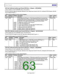
ADC Gain Calibration Temperature Sensor Channel Register—ADCGAINTEMPSENS
Address 0x00002238, Reset: 0x00004000, Name: ADCGAINTEMPSENS
The ADCGAINTEMPSENS register provides the ADC gain calibration value used when measuring the internal temperature sensor.
Table 70. Bit Descriptions for ADCGAINTEMPSENS Register
Bits
[31:15] Reserved
[14:0] GAINTEMPSENS
Bit Name
Settings
Description
Reset
0x0
Access
R
Reserved.
Gain calibration for the temperature sensor channel. These bits provide ADC gain
correction for the temperature sensor channel. This value is stored as a signed
number. Bit 14 is the sign bit and Bits[13:0] represent the fractional part.
0x4000
R/W
0x0000 0. Illegal value resulting in an ADC result of 0.
0x2000 0.5. ADC result multiplied by 0.5.
0x4000 1.0. ADC result multiplied by 1. No gain adjustment (default value).
0x4001 1.000061. Minimum positive gain adjustment.
0x7FFF 2. Maximum positive gain adjustment.
0x0001 0.000061. Maximum negative gain adjustment.
0x3FFF 0.999939. Minimum negative gain adjustment.
ADC DIGITAL POSTPROCESSING REGISTERS (OPTIONAL)
Table 71. ADC Digital Postprocessing Registers Summary
Address
Name
Description
Reset
Access
0x000020A8
0x000020AC
0x000020B0
0x000020B4
0x000020B8
ADCMIN
ADCMINSM
ADCMAX
ADCMAXSMEN
ADCDELTA
ADC minimum value check register
ADC minimum hysteresis value register
ADC maximum value check register
ADC maximum hysteresis value register
ADC delta value check register
0x00000000
0x00000000
0x00000000
0x00000000
0x00000000
R/W
R/W
R/W
R/W
R/W
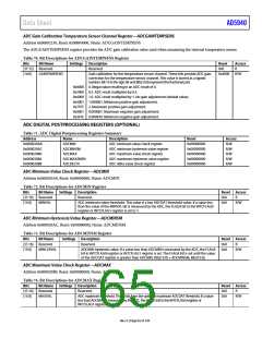
ADC Minimum Value Check Register—ADCMIN
Address 0x000020A8, Reset: 0x00000000, Name: ADCMIN
Table 72. Bit Descriptions for ADCMIN Register
Bits
[31:16] Reserved
[15:0] MINVAL
Bit Name
Settings Description
Reset Access
Reserved.
0x0
0x0
R
ADC minimum value threshold. This value is a low ADCDAT threshold value. If a value less
than the value of the MINVAL bit is measured by the ADC, the FLAG4 bit in the INTCFLAG0
register or INTCFLAG1 register is set to 1.
R/W
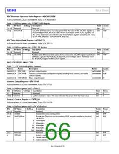
ADC Minimum Hysteresis Value Register—ADCMINSM
Address 0x000020AC, Reset: 0x00000000, Name: ADCMINSM
Table 73. Bit Descriptions for ADCMINSM Register
Bits
[31:16] Reserved
[15:0] MINCLRVAL
Bit Name
Settings Description
Reset Access
Reserved.
0x0
0x0
R
ADCMIN hysteresis value. If a value less than ADCMIN is measured by the ADC, the FLAG4
R/W
bit in INTCFLAG0 register or INTCFLAG1 register is set. The FLAG4 bit is set until the value
of the ADCDAT register is greater than ADCMIN, Bits[15:0] + ADCMINSM, Bits[15:0].
ADC Maximum Value Check Register—ADCMAX
Address 0x000020B0, Reset: 0x00000000, Name: ADCMAX
Table 74. Bit Descriptions for ADCMAX Register
Bits
[31:16] Reserved
[15:0] MAXVAL
Bit Name
Settings Description
Reset Access
Reserved.
0x0
0x0
R
ADC maximum threshold. These bits form the optional maximum ADCDAT threshold. If a value
R/W
less than ADCMAX is measured by the ADC, the FLAG5 bit in the INTCFLAG0 register or
INTCFLAG1 register is set to 1.
Rev. 0 | Page 65 of 130

 ADI [ ADI ]