AD5940
Data Sheet
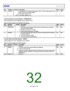
Bits
[11:0]
Bit Name
DACIN12
Settings Description
Reset Access
Low power DAC 12-bit output data register (1 LSB = 537 µV). A value between 0 and 0x0
0xFFF sets the 12-bit output voltage.
Sets output voltage to 0.2 V.
0xFFF Sets output voltage to 2.4 V.
R/W
0
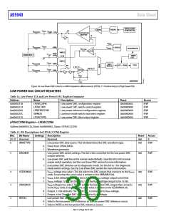
Low Power Reference Control Register—LPREFBUFCON
Address 0x00002050, Reset: 0x00000000, Name: LPREFBUFCON
Table 18. Bit Descriptions for LPREFBUFCON Register
Bits
Bit Name
Settings Description
Reset Access
[31:2] Reserved
Reserved.
0x0
0x0
R
R/W
1
0
LPBUF2P5DIS
Low power output band gap buffer. This bit is normally cleared to enable the
low power reference buffer.
Enables the low power 2.5 V buffer.
Powers down the low power 2.5 V buffer.
0
1
LPREFDIS
Low power band gap power-down bit. This bit is normally cleared to enable the
low power reference.
0x0
R/W
0
1
Low power reference enabled.
Low power reference powered down.
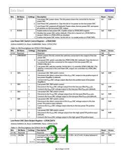
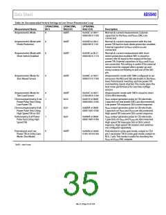
Common-Mode Switch Mux Register—SWMUX
Address 0x0000235C, Reset: 0x00000000, Name: SWMUX
Table 19. Bit Descriptions for SWMUX Register
Bits
Bit Name
Settings Description
Reset Access
[31:4] Reserved
Reserved.
0x0
0x0
R
R/W
3
CMMUX
Common-mode resistor select for AIN2 pin and AIN3 pin.
0
1
Common-mode switch off.
Enables the common-mode switches with a 10 MΩ resistor to set up the common-mode
voltage on the AIN2 and AIN3 pins. The voltage is driven by the low power TIA and the
AIN4/LPF0 pin.
[2:0]
Reserved
Reserved.
0x0
R/W
Rev. 0 | Page 32 of 130

 ADI [ ADI ]