Data Sheet
AD5940
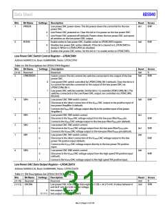
Bits
1
Bit Name
PWDEN
Settings Description
Low power DAC power-down. This bit powers down the control bit for the low
Reset Access
0x1
R/W
power DAC.
0
1
Low Power DAC powered on. Clear this bit to 0 to power on the low power DAC.
Low Power DAC powered off (default). Powers down the low power DAC and opens
all switches on the low power DAC output.
0
RSTEN
Enable writes to low power DAC. Enables writes to LPDACDAT0 register.
0x0
R/W
0
1
Disables low power DAC writes (default). If this bit is cleared to 0, LPDACDAT0 is
always 0. Writes to LPDACDAT0 are disabled.
Enables low power DAC writes. Set this bit to 1 to enable writes to LPDACDAT0.
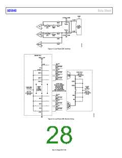
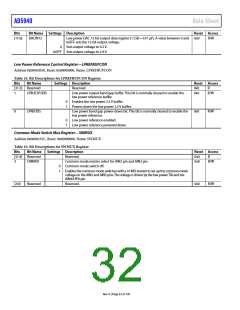
Low Power DAC Switch Control Register—LPDACSW0
Address 0x00002124, Reset: 0x00000000, Name: LPDACSW0
Table 16. Bit Descriptions for LPDACSW0 Register
Bits
Bit Name
Settings Description
Reset Access
[31:6] Reserved
Reserved.
0x0
0x0
R
5
4
LPMODEDIS
Switch control. This bit controls the switches connected to the output of the low
power DAC.
R/W
0
1
Low power DAC switch controlled by LPDACCON0, Bit 5 (default). Clear this bit to 0
to control the switches connected to the output of the low power DAC via
LPDACCON0, Bit 5.
Low power DAC switches override. Set this bit to 1 to overrides LPDACCON0, Bit 5. The
switches connected to the Low Power DAC output are controlled via LPDACSW0,
Bits[4:0].
Low power DAC SW4 switch control.
Disconnects the direct connection of the VBIAS0 DAC output to the positive input of
low power Amplifier 0 (default).
Connects the VBIAS0 DAC voltage output directly to the positive input of low power
Amplifier 0.
Low power DAC SW3 switch control.
Disconnects the VBIAS0 DAC voltage output from the low-pass filter/VBIAS0 pin.
Connects the VBIAS0 DAC voltage output to the low-pass filter/VBIAS0 pin (default).
Low power DAC SW2 switch control.
Disconnects the VZERO0 DAC voltage output from the low-pass filter/VZERO0 pin.
Connects the VZERO0 DAC voltage output to the low-pass filter/VZERO0 pin (default).
Low power DAC SW1 switch control.
SW4
0x0
0x1
R/W
0
1
3
2
1
SW3
SW2
SW1
0
1
R/W
R/W
R/W
0
1
0x1
0x0
0
1
Disconnects the direct connection of the VZERO0 DAC voltage output to the low
power TIA positive input (default).
Connects the VZERO0 DAC voltage output directly to the low power TIA positive
input.
0
SW0
Low power DAC SW0 switch control.
0x0
0
1
Disconnects the VZERO0 DAC voltage output from the high speed TIA positive input
(default).
Connects the VZERO0 DAC voltage output to the high speed TIA positive input.
R/W
Low Power DAC Data Output Register—LPDACDAT0
Address 0x00002120, Reset: 0x00000000, Name: LPDACDAT0
Table 17. Bit Descriptions for LPDACDAT0 Register
Bits
Bit Name
Settings Description
Reset Access
[31:18] Reserved
[17:12] DACIN6
Reserved.
0x0
0x0
R
Low power DAC 6-bit output data register (1 LSB = 34.375 mV). A value between 0
R/W
and 0x3F sets the 6-bit output voltage.
0
Sets output voltage to 0.2 V.
111111 Sets output voltage to 2.366 V.
Rev. 0 | Page 31 of 130

 ADI [ ADI ]