AD5940
Data Sheet
WAVEFORM
GENERATOR
HSDAC
GAIN
C
C
D5
ISO1
R
R
R
LIMIT
ACCESS1
CE0
EXCITATION
BUFFER
N
P
P5
V
BIAS
ISO3
AIN2
ACCESS3
LPDAC0
V
ZERO
SEQUENCER
R
FILTER
+
LSTIA
–
10MΩ
AIN4/
LPF0
C
LPF
UNKNOWN Z
16MHz
OSC
VCM
10MΩ
C
C
ISO4
R
R
AIN3
AIN1
ACCESS4
ADC/
800kHz
DFT = 2048
FIFO
N2
1.1V
+
HSTIA_P
ISO2
HSTIA
ACCESS2
–
T2
T9
R
TIA
AD5940
C
TIA
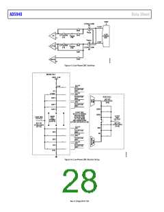
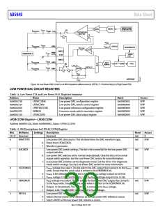
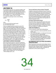
Figure 18. Low Power DACs Used in a 4-Wire Impedance Measurement (HSTIA_P = Positive Output of High Speed TIA)
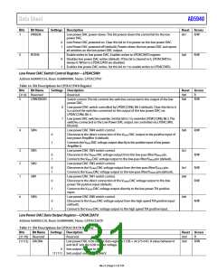
LOW POWER DAC CIRCUIT REGISTERS
Table 14. Low Power TIA and Low Power DAC Registers Summary
Address
Name
Description
Reset
Access
R/W
R/W
R/W
R/W
0x00002128
0x00002124
0x00002050
0x0000235C
0x00002120
LPDACCON0
LPDACSW0
LPREFBUFCON
SWMUX
Low power DAC configuration register
Low power DAC switch control register
Low power reference configuration register
Common-mode switch mux select register
Low power DAC data output register
0x00000002
0x00000000
0x00000000
0x00000000
0x00000000
LPDACDAT0
R/W
LPDACCON0 Register—LPDACCON0
Address 0x00002128, Reset: 0x00000002, Name: LPDACCON0
Table 15. Bit Descriptions for LPDACCON0 Register
Bits
Bit Name
Settings Description
Reset Access
[31:7] Reserved
Reserved.
0x0
0x0
R
R/W
6
5
WAVETYPE
DACMDE
Low power DAC data source. This bit determines the DAC waveform type.
Direct from LPDACDAT0.
Waveform generator.
0
1
Low power DAC switch settings. This bit is the control bit for the low power DAC
output switches.
0x0
R/W
0
1
Low power DAC switches set for normal mode (default). Clear this bit to 0 for normal
output switch operation. See the Low Power DAC section for more information.
Low power DAC switches set for diagnostic mode. Set this bit to 1 for diagnostic
mode switch settings. See the Low Power DAC section for more information.
4
3
2
VZEROMUX
VBIASMUX
REFSEL
VZERO0 voltage mux select. This bit selects the DAC output that connects to the VZERO0
node. Ensure that the same value is written to the VBIASMUX bit.
VZERO0, 6-bit (default). Clear this bit to 0 for the VZERO0 voltage output to be 6-bit.
VZERO0, voltage 12-bit. Set this bit to 1 for the VZERO0 voltage output to be 12-bit.
0x0
0x0
0x0
R/W
R/W
R/W
0
1
VBIAS0 voltage mux select. This bit selects the low power DAC output that connects
to the VBIAS0 node. Ensure that the same value is written to the VZEROMUX bit.
Output, 12-bit (default). The 12-bit DAC is connected to VBIAS0 voltage.
Output, 6-bit. The 6-bit DAC is connected to VBIAS0 voltage.
Low power DAC reference select.
0
1
0
1
Selects the low power 2.5 V reference as the low power DAC reference source.
Selects AVDD as the low power DAC reference source.
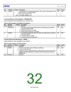
Rev. 0 | Page 30 of 130

 ADI [ ADI ]