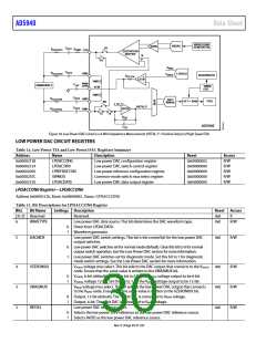
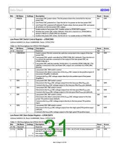
AD5940
Data Sheet
LOW POWER TIA
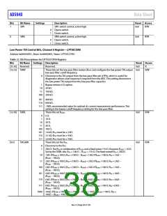
The AD5940 has a low power TIA channel that amplifies small
current inputs to voltages to be measured by the ADC. The load
resistor and gain resistor are internal and programmable. Select the
Current-Limit Feature of the Low Power TIA and PA
In addition to the protection diode, the low power TIA also has
a built in current limiting feature. If the current sourced or sunk
from the low power TIA is greater than the overcurrent limit
protection specified in Table 1, the amplifiers clamp the current
to this limit. If a sensor attempts to source or sink more than
the overcurrent limit during startup, the amplifier clamps the
output current. Do not use this feature more frequently or for
longer than specified in Table 1.
RTIA value that maximizes the ADC input range of 900 mV
when PGA gain is 1 or 1.5. Refer to the Specifications section
for the maximum voltage for other PGA settings.
To calculate the required gain resistor, use the following
equation:
0.9 V
RTIA
IMAX
=
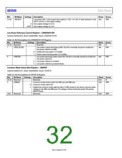
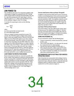
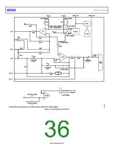
Low Power TIA Force/Sense Feature
The LPTIACON0[9:5] bits select different gain resistor values
for the low power TIA, labeled as RTIA in Figure 19. The force
and sense connections shown on the feedback path of the low
power TIA are used to avoid voltage (I × R) drops on the switches,
where:
MAX is the expected full-scale input current.
TIA is the required gain resistor.
I
R
There are a number of switches around the low power TIA
circuitry. The LPTIASW0 register configures these switches.
Figure 19 shows the available switches. When the TIAGAIN bits
(Bits[9:5]) in the LPTIACON0 register are set, these switches
are closed automatically. When these switches are closed, there
is a force/sense circuit with a low-pass filter resistor (RLPF) and a
capacitor on the AIN4/LPF0 pin that acts as a resistor-capacitor
(RC) delay circuit. The LPTIA0_P_LPF0 connects the output of
the low power TIA low-pass filter to the ADC mux. Analog
Devices recommends that the LPTIA0_P_LPF0 mux option be
selected as the ADC input when using the low power TIA. It is
recommended to connect a 100 nF capacitor between the
RC0_0 pin and the RC0_1 pin to stabilize the low power TIA.
which select different RTIA settings for the internal RTIA
.
USING AN EXTERNAL RTIA
To use an external RTIA resistor, take the following steps:
1. Connect an external RTIA resistor across the RC0_0 pin and
the RC0_1 pin.
2. Clear LPTIACON0, Bits[9:5] = 0 to disconnect the internal
RTIA resistor from the TIA output terminal.
3. Close the SW9 switch by setting LPTIASW0, Bit 9 = 1.
When using the internal RTIA reisistor, open the SW9 switch.
4. Connect an external capacitor in parallel with an external
RTIA resistor to maintain loop stability. The recommended
value of this external capacitor is 100 nF.
LOW POWER TIA PROTECTION DIODES
RECOMMENDED SWITCH SETTINGS FOR VARIOUS
OPERATING MODES
Back to back protection diodes are connected in parallel with
the RTIA resistor. These diodes are connected or disconnected by
closing or opening SW0, controlled by LPTIASW0, Bit 0.These
diodes are intended for use when switching RTIA gain settings to
amplify small currents to prevent saturation of the TIA. These
diodes have a leakage current specification dependent on the
voltage across the diodes. If the differential voltage across the
diodes is >200 mV, leakage can be >1 nA. If the voltage is
>500 mV, leakage can be >1 μA.
Table 20 describes the recommended switch settings in the low
power potentiostat loop for various measurement types. For all
measurement types, setting the switch to 1 closes the switch and
setting the switch to 0 opens the switch. LPTIASW0[13:0]
controls SW13 to SW0, as shown in Figure 19.
Rev. 0 | Page 34 of 130

 ADI [ ADI ]