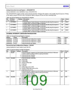
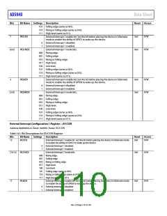
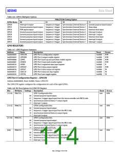
Data Sheet
AD5940
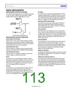
DIGITAL INPUTS/OUTPUTS
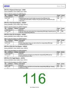
Bit Toggle
DIGITAL INPUTS/OUTPUTS FEATURES
The GP0 port has a corresponding bit toggle register, GP0TGL.
Using the bit toggle register, it is possible to invert one or more
GPIO data outputs without affecting other outputs within the
port. Only the GPIOx pin that corresponds to the write data bit
equal to 1 is toggled. The remaining GPIOs are unaffected.
The AD5940 features eight GPIO pins. The GPIOs are grouped
in one port, which is eight bits wide. Each GPIOx contains
multiple functions that are configurable by user code.
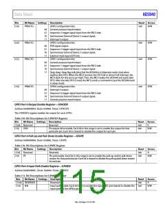
OUTPUT ENABLE
GP0OEN
Input/Output Data Output Enable
OUTPUT DATA
The GP0 port has a data output enable register, GP0OEN, by
which the data output path is enabled. When the data output
enable register bits are set, the values in GP0OUT are reflected
on the corresponding GPIOx pins.
GP0OUT, GP0SET,
GP0CLR, GP0TGL
GPIO
INPUT ENABLE
GP0IEN
Interrupt Inputs
Each GPIOx pin can be configured to react to external events.
These events can be detected and used to wake up the device or
to trigger specific sequences. These events are configured in the
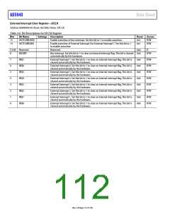
EIxCON register. Writing to the corresponding bit in the EICLR
register clears the interrupt flag. For further information, see
the Interrupts section.
INPUT DATA
GP0IN
Figure 48. Digital Input/Output Diagram
DIGITAL INPUTS/OUTPUTS OPERATION
Input/Output Pull-Up Enable
Interrupt Outputs
GPIO0, GPIO1, GPIO3, GPIO4, GPIO5, GPIO6, and GPIO7
pins have pull-up resistors that are enabled or disabled using the
GP0PE register. Unused GPIOs must have the respective pull-up
resistors disabled to reduce power consumption.
The AD5940 has two external interrupts that can be mapped to
certain GPIOx pins (see the GP0CON register). When an
interrupt occurs, the AD5940 sets the GPIOx pin high. When
the interrupt is cleared, the AD5940 brings the GPIOx pin low.
These interrupts are configured in the interrupt controller
register (see the Interrupts section).
Input/Output Data Input
When the GPIOs are configured as inputs using the GP0IEN
register, the GPIO input levels are available in the GP0IN register.
Digital Port Multiplex
Input/Output Data Output
The digital port multiplex block provides control over the GPIO
functionality of the specified pins. These options are configured
in the GP0CON register.
When the GPIOs are configured as outputs, the values in the
GP0OUT register are reflected on the GPIOs.
Bit Set
GPIOx Control with the Sequencer
The GP0 port has a corresponding bit set register, GP0SET.
Using the bit set register, it is possible to set one or more GPIO
data outputs without affecting other outputs within the port.
Only the GPIOx corresponding to the write data bit equal to 1
is set. The remaining GPIOs are unaffected.
Each GPIOx on the AD5940 can be controlled via the sequencer.
This control allows syncing of external devices during timing
critical applications using a dedicated register, SYNCEXTDEVICE.
To control the GPIOs via this register, the GPIOx must first be
configured as an output in the GP0OEN register and sync must
be selected in the GP0CON register.
Bit Clear
The GP0 port has a corresponding bit clear register, GP0CLR.
Use the bit clear register to clear one or more GPIO data
outputs without affecting other outputs within the port. Only
the GPIOx that corresponds to the write data bit equal to 1 is
cleared. The remaining GPIOs are unaffected.
Rev. 0 | Page 113 of 130

 ADI [ ADI ]