ADSP-BF542/ADSP-BF544/ADSP-BF547/ADSP-BF548/ADSP-BF549
HOSTDP A/C Timing-Host Write Cycle
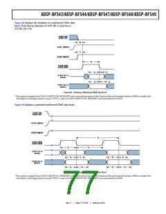
Table 55 and Figure 46 describe the HOSTDP A/C host write
cycle timing requirements.
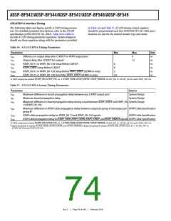
Table 55. Host Write Cycle Timing Requirements
Parameter
Min
Max
Unit
Timing Requirements
tSADWRL
tHADWRH
tWRWL
HOST_ADDR/HOST_CE Setup Before HOST_WR Falling Edge
HOST_ADDR/HOST_CE Hold After HOST_WR Rising Edge
HOST_WR Pulse Width Low (ACK Mode)
4
ns
ns
ns
ns
ns
2.5
tDRDYWRL + tRDYPRD + tDWRHRDY
1.5 × tSCLK + 8.7
HOST_WR Pulse Width Low (INT Mode)
tWRWH
HOST_WR Pulse Width High or Time Between HOST_WR Rising Edge 2 × tSCLK
and HOST_RD Falling Edge
tDWRHRDY
tHDATWH
tSDATWH
HOST_WR Rising Edge Delay After HOST_ACK Rising Edge(ACKMode) 0
ns
ns
ns
HOST_D15–0 Hold After HOST_WR Rising Edge
HOST_D15–0 Setup Before HOST_WR Rising Edge
2.5
3.5
Switching Characteristics
tDRDYWRL HOST_ACK Falling Edge After HOST_CE Asserted (ACK Mode)
tRDYPWR HOST_ACK Low Pulse-Width for Write Access (ACK Mode)
11.25
NM1
ns
ns
1 NM (not measured)—This parameter is based on tSCLK. It is not measured because the number of SCLK cycles for which HOST_ACK remains low depends on the Host DMA
FIFO status. This is system design dependent.
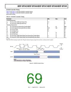
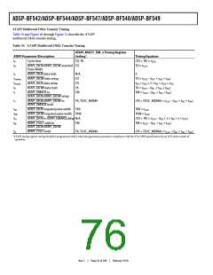
HOST_ADDR
HOST_CE
tSADWRL
tHADWRH
tWRWH
tWRWL
HOST_WR
HOST_DATA
HOST_ACK
tSDATWH
tHDATWH
tRDYPWR
tDRDYWRL
tDWRHRDY
In Figure 46, HOST_DATA is HOST_D0–D15.
Figure 46. HOSTDP A/C- Host Write Cycle
Rev. C
|
Page 73 of 100
|
February 2010

 ADI [ ADI ]