ADSP-BF542/ADSP-BF544/ADSP-BF547/ADSP-BF548/ADSP-BF549
SD/SDIO Controller Timing
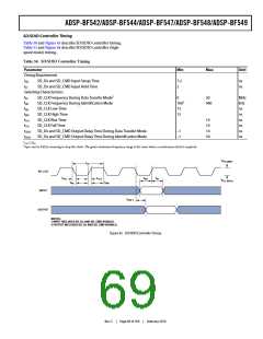
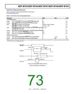
Table 50 and Figure 43 describe SD/SDIO controller timing.
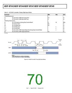
Table 51 and Figure 44 describe SD/SDIO controller (high-
speed mode) timing.
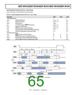
Table 50. SD/SDIO Controller Timing
Parameter
Min
Max
Unit
Timing Requirements
tISU
tIH
SD_Dx and SD_CMD Input Setup Time
SD_Dx and SD_CMD Input Hold Time
7.2
2
ns
ns
Switching Characteristics
fPP
fOD
tWL
tWH
SD_CLK Frequency During Data Transfer Mode1
SD_CLK Frequency During Identification Mode
SD_CLK Low Time
0
20
400
MHz
kHz
ns
1002
15
15
SD_CLK High Time
ns
tTLH
tTHL
SD_CLK Rise Time
SD_CLK Fall Time
SD_Dx and SD_CMD Output Delay Time During Data Transfer Mode
SD_Dx and SD_CMD Output Delay Time During Identification Mode
10
10
14
50
ns
ns
ns
ns
tODLY
tODLY
1 tPP=1/fPP
–1
–1
2 Spec can be 0 kHz, meaning to stop the clock. The given minimum frequency range is for cases where a continuous clock is required.
VOH (MIN)
tPP
SD_CLK
tTHL
tTLH
tISU
tIH
VOL (MAX)
tWL
tWH
INPUT
tODLY
OUTPUT
NOTES:
1 INPUT INCLUDES SD_Dx AND SD_CMD SIGNALS.
2 OUTPUT INCLUDES SD_Dx AND SD_CMD SIGNALS.
Figure 43. SD/SDIO Controller Timing
Rev. C
|
Page 69 of 100
|
February 2010

 ADI [ ADI ]