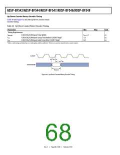
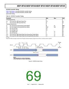
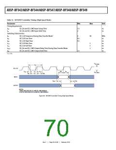
ADSP-BF542/ADSP-BF544/ADSP-BF547/ADSP-BF548/ADSP-BF549
Timer Cycle Timing
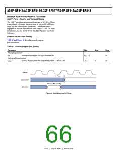
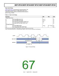
Table 48 and Figure 41 describe timer expired operations. The
input signal is asynchronous in “width capture mode” and
“external clock mode” and has an absolute maximum input fre-
quency of (fSCLK/2) MHz.
Table 48. Timer Cycle Timing
Parameter
Min
Max
Unit
Timing Characteristics
tWL
tWH
tTIS
tTIH
Timer Pulse Width Input Low1
tSCLK +1
tSCLK +1
6.5
ns
ns
ns
ns
Timer Pulse Width Input High1
Timer Input Setup Time Before CLKOUT Low2
Timer Input Hold Time After CLKOUT Low2
–1
Switching Characteristics
tHTO
Timer Pulse Width Output
1×tSCLK
(232 – 1)×tSCLK ns
ns
tTOD
Timer Output Delay After CLKOUT High
6
1 The minimum pulse widths apply for TMRx signals in width capture and external clock modes.
2 Either a valid setup and hold time or a valid pulse width is sufficient. There is no need to resynchronize timer flag inputs.
CLKOUT
tTOD
TMRx OUTPUT
tTIS
tTIH
tHTO
TMRx INPUT
tWH,tWL
Figure 41. Timer Cycle Timing
Rev. C
|
Page 67 of 100
|
February 2010

 ADI [ ADI ]