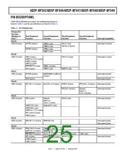
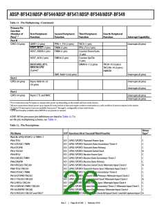
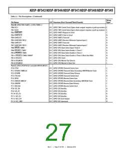
ADSP-BF542/ADSP-BF544/ADSP-BF547/ADSP-BF548/ADSP-BF549
The assembly language, which takes advantage of the proces-
(EE-68) on the Analog Devices web site under
sor’s unique architecture, offers the following advantages:
www.analog.com/ee-notes. This document is updated regularly
to keep pace with improvements to emulator support.
• Seamlessly integrated DSP/MCU features are optimized for
both 8-bit and 16-bit operations.
• A multi-issue load/store modified-Harvard architecture,
which supports two 16-bit MAC or four 8-bit ALU + two
load/store + two pointer updates per cycle.
• All registers, I/O, and memory are mapped into a unified
4G byte memory space, providing a simplified program-
ming model.
• Microcontroller features, such as arbitrary bit and bit-field
manipulation, insertion, and extraction; integer operations
on 8-, 16-, and 32-bit data-types; and separate user and
supervisor stack pointers.
MXVR BOARD LAYOUT GUIDELINES
The MXVR Loop Filter RC network is connected between the
MLF_P and MLF_M pins in the following manner:
Capacitors:
• C1: 0.047 µF (PPS type, 2% tolerance recommended)
• C2: 330 pF (PPS type, 2% tolerance recommended)
Resistor:
• R1: 330 Ω (1% tolerance)
The RC network should be located physically close to the
MLF_P and MLF_M pins on the board.
The RC network should be shielded using GNDMP traces.
Avoid routing other switching signals near the RC network to
avoid crosstalk.
• Code density enhancements, which include intermixing of
16- and 32-bit instructions (no mode switching, no code
segregation). Frequently used instructions are encoded in
16 bits.
MXI driven with external clock oscillator IC:
DEVELOPMENT TOOLS
• MXI should be driven with the clock output of a clock
oscillator IC running at a frequency of 49.152 MHz or
45.1584 MHz.
The ADSP-BF54x Blackfin processors are supported with a
complete set of CROSSCORE® software and hardware develop-
ment tools, including Analog Devices emulators and
VisualDSP++® development environment. The same emulator
hardware that supports other Blackfin processors also fully
emulates the ADSP-BF54x Blackfin processors.
• MXO should be left unconnected.
• Avoid routing other switching signals near the oscillator
and clock output trace to avoid crosstalk. When not possi-
ble, shield traces with ground.
EZ-KIT Lite Evaluation Board
MXI/MXO with external crystal:
• The crystal must be a fundamental mode crystal running at
a frequency of 49.152 MHz or 45.1584 MHz.
• The crystal and load capacitors should be placed physically
close to the MXI and MXO pins on the board.
• Board trace capacitance on each lead should not be more
than 3 pF.
• Trace capacitance plus load capacitance should equal the
load capacitance specification for the crystal.
• Avoid routing other switching signals near the crystal and
components to avoid crosstalk. When not possible, shield
traces and components with ground.
For evaluation of ADSP-BF54x Blackfin processors, use the
ADSP-BF548 EZ-KIT Lite® board available from Analog
Devices. Order part number ADZS-BF548-EZLITE. The board
comes with on-chip emulation capabilities and is equipped to
enable software development. Multiple daughter cards are
available.
DESIGNING AN EMULATOR-COMPATIBLE
PROCESSOR BOARD
The Analog Devices family of emulators are tools that every sys-
tem developer needs to test and debug hardware and software
systems. Analog Devices has supplied an IEEE 1149.1 JTAG test
access port (TAP) on each JTAG processor. The emulator uses
the TAP to access the internal features of the processor, allow-
ing the developer to load code, set breakpoints, observe
variables, observe memory, and examine registers. The proces-
sor must be halted to send data and commands, but once an
operation has been completed by the emulator, the processor is
set running at full speed with no impact on system timing.
To use these emulators, the target board must include a header
that connects the processor’s JTAG port to the emulator.
For details on target board design issues including mechanical
layout, single processor connections, multiprocessor scan
chains, signal buffering, signal termination, and emulator pod
logic, see Analog Devices JTAG Emulation Technical Reference
V
DDMP/GNDMP—MXVR PLL power domain:
• Route VDDMP and GNDMP with wide traces or as isolated
power planes.
• Drive VDDMP to same level as VDDINT
• Place a ferrite bead between the VDDINT power plane and the
VDDMP pin for noise isolation.
.
• Locally bypass VDDMP with 0.1 µF and 0.01 µF decoupling
capacitors to GNDMP
.
• Avoid routing switching signals near to VDDMP and GNDMP
traces to avoid crosstalk.
Rev. C
|
Page 23 of 100
|
February 2010

 ADI [ ADI ]