ADL5513
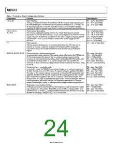
CONTROLLER MODE
CONSTANT POWER OPERATION
The ADL5513 provides a controller mode feature at Pin VOUT.
Using VSET for the setpoint voltage, it is possible for the ADL5513
to control subsystems, such as power amplifiers (PAs), variable
gain amplifiers (VGAs), or variable voltage attenuators (VVAs),
which have output power that increases monotonically with
respect to their gain control signal.
In controller mode, the ADL5513 can be used to hold the output
power stable over a broad temperature/input power range. This
can be useful in topologies where a transmit card is driving an
HPA or when connecting power-sensitive modules together.
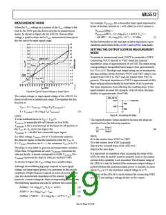
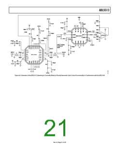
Figure 44 shows a schematic of a circuit setup that holds the
output power to approximately −39 dBm at 900 MHz when the
input power is varied over a 62 dB dynamic range. Figure 43
shows the performance results. A portion of the output power is
coupled to the input of ADL5513 using a 20 dB coupler. The
VSET voltage is set to 0.65 V, which forces the ADL5513 output
voltage to control the ADL5330 to deliver −59 dBm. (If the
ADL5513 is in measurement mode and a −59 dBm input power
is applied, the output voltage is 0.65 V). A generic op amp is used
(AD8062) to invert the slope of the ADL5513 so that the gain of
the ADL5330 decreases as the ADL5513 control voltage
increases. The high end power is limited by the maximum gain
of the ADL5330 and can increase if VSET is moved so that the
ADL5513 has a higher power on its input and a VGA with
higher linearity is used. The low power is limited by the
sensitivity of the ADL5513 and can be increased with a reduction
in the coupling value of the coupler.
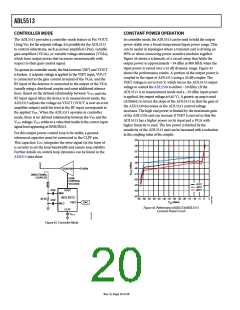
To operate in controller mode, the link between VSET and VOUT
is broken. A setpoint voltage is applied to the VSET input, VOUT
is connected to the gain control terminal of the VGA, and the
RF input of the detector is connected to the output of the VGA
(usually using a directional coupler and some additional attenua-
tion). Based on the defined relationship between VOUT and the
RF input signal when the device is in measurement mode, the
ADL5513 adjusts the voltage on VOUT (VOUT is now an error
amplifier output) until the level at the RF input corresponds to
the applied VSET. When the ADL5513 operates in controller
mode, there is no defined relationship between the VSET and the
VOUT voltage; VOUT settles to a value that results in the correct input
signal level appearing at INHI/INLO.
For this output power control loop to be stable, a ground-
referenced capacitor must be connected to the CLPF pin.
This capacitor, CFLT, integrates the error signal (in the form of
a current) to set the loop bandwidth and ensure loop stability.
Further details on control loop dynamics can be found in the
AD8315 data sheet.
–35
–36
–37
–38
–39
–40
–41
–42
VGA/VVA
RFIN
DIRECTIONAL
COUPLER
GAIN
CONTROL
VOLTAGE
+25°C
–40°C
+85°C
–43
–44
–45
47nF
47nF
VOUT
INHI
ADL5513
52.3Ω
–65 –60 –55 –50 –45 –40 –35 –30 –25 –20 –15 –10 –5
0
5
P
(dBm)
VSET
DAC
IN
INLO
Figure 43. Performance of ADL5330/ADL5513
Constant Power Circuit
CLPF
C
FLT
Figure 42. Controller Mode
Rev. 0 | Page 20 of 28

 ADI [ ADI ]