ADL5513
2.50
2.25
2.00
1.75
1.50
1.25
1.00
0.75
0.50
0.25
0
2.5
improve linearity and extend the dynamic range, unless enough
calibration points are used to remove error.
2.0
1.5
Figure 34 is a useful tool for estimating temperature drift at a
particular power level with respect to the (nonideal) output
voltage at ambient.
1.0
0.5
0
TEMPERATURE COMPENSATION OF OUTPUT
VOLTAGE
–0.5
–1.0
–1.5
–2.0
–2.5
The primary component of the variation in VOUT vs. temperature as
the input signal amplitude is held constant is the drift of the
intercept. This drift is also a weak function of the input signal
frequency; therefore, a provision is made for the optimization of
the internal temperature compensation at a given frequency by
providing Pin TADJ with dual functionality. The first function
for this pin is temperature compensation and the second function
is to power down the device when VTADJ = VPOS − 0.3 V (see the
Power-Down Functionality section).
+25°C
–40°C
+85°C
+125°C
–70 –65 –60 –55 –50 –45 –40 –35 –30 –25 –20 –15 –10 –5
0
5 10
P
(dBm)
IN
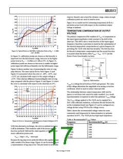
Figure 33. Typical Device at 3600 MHz, Calibration Points at PIN = −12 dBm
and −40 dBm
In Figure 32, calibration points are chosen so that linearity is
improved over the full dynamic range, but error at the higher
power level at PIN = −10 dBm is 0.5 dB at 25°C. In Figure 33,
calibration points are chosen so that error is smaller at higher
power input ,but with loss of linearity over the full dynamic range.
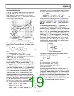
V
INTERNAL
I
COMP
PWDN/TADJ
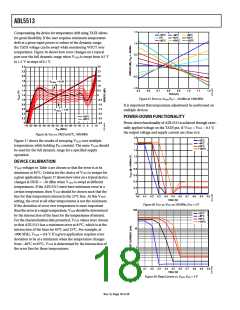
Figure 34 shows another way of presenting the error of a log
amp detector. The same typical device from Figure 32 and
Figure 33 is presented where the error at −40°C, +85°C, and
+125°C are calculated with respect to the output voltage at
+25°C. This is the key difference in presenting the error of a log
amp compared with the plots in Figure 32 and Figure 33 where
the error is calculated with respect to the ideal line at 25°C.
COMM
COMM
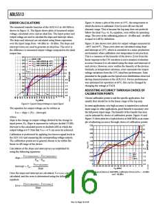
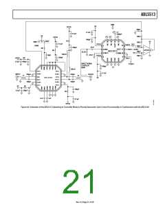
Figure 35. TADJ Interface
VTADJ is a voltage forced between TADJ and ground. The value
of this voltage determines the magnitude of an analog correction
coefficient, which is used to reduce intercept drift.
2.50
2.25
2.00
1.75
1.50
1.25
1.00
0.75
0.50
0.25
0
2.5
–40°C
+85°C
+125°C
2.0
The relationship between output temperature drift and fre-
quency is not linear and cannot be easily modeled. As a result,
experimentation is required to select the optimum VTADJ voltage.
1.5
1.0
0.5
The VTADJ voltage applied to Pin TADJ can be supplied by a
DAC with sufficient resolution, or Resistor R8 and Resistor R9
on the evaluation board (see Figure 47) can be configured as a
voltage divider using VPOS as the voltage source.
0
–0.5
–1.0
–1.5
–2.0
–2.5
Table 4 shows the recommended voltage values for some
commonly used frequencies in characterization to optimize
operation at 85°C. The TADJ pin has high input impedance.
–70 –65 –60 –55 –50 –45 –40 –35 –30 –25 –20 –15 –10 –5
0
5 10
P
(dBm)
IN
Table 4. Recommended VTADJ Values
Figure 34. Error vs. Temperature with Respect to Output Voltage at 25°C,
3600 MHz
Frequency
100 MHz
900 MHz
1.9 GHz
Recommended VTADJ (V)
0.89
0.86
0.80
0.84
0.83
0.90
With this alternative technique, the error at ambient becomes
0 dB by definition. This would be valid if the device transfer
function perfectly followed the ideal equation or if there were
many calibration points used.
2.14 GHz
2.6 GHz
VOUT = Slope × (PIN − Intercept)
3.6 GHz
Because the log amp never perfectly follows this equation, espe-
cially outside of its linear range, Figure 34 can be misleading as
a representation of log amp error. This plot tends to artificially
Rev. 0 | Page 17 of 28

 ADI [ ADI ]