ADL5513
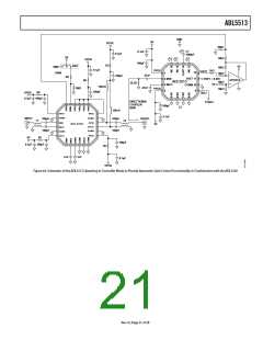
Due to the amplification of out-of-band noise by AD8368, a
band-pass filter was inserted between the AD8368 and ADL5513
to increase the low end sensitivity. The VGA amplifies low power
signals and attenuates high power signals to fit them in the
detectable range of the ADL5513. If an amplifier with higher
gain and lower noise figure is used, better than 90 dB sensitivity
can be achieved for use in an RSSI application.
INCREASING THE DYNAMIC RANGE OF THE
ADL5513
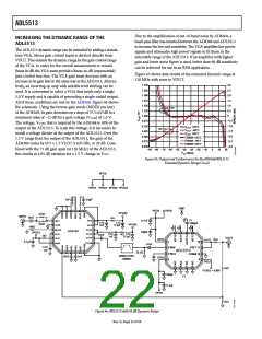
The ADL5513 dynamic range can be extended by adding a standa-
lone VGA, whose gain control input is derived directly from
VOUT. This extends the dynamic range by the gain control range
of the VGA. In order for the overall measurement to remain
linear in dB, the VGA must provide a linear-in-dB (exponential)
gain control function. The VGA gain must decrease with an
increase in its gain bias in the same way as the ADL5513. Alterna-
tively, an inverting op amp with suitable level shifting can be
used. It is convenient to select a VGA that needs only a single
5.0 V supply and is capable of generating a single-ended output.
All of these conditions are met by the AD8368. Figure 46 shows
the schematic. Using the inverse gain mode (MODE pin low)
of the AD8368, its gain decreases on a slope of 37.5 mV/dB to a
minimum value of −12 dB for a gain voltage (VGAIN) of 1.0 V.
The voltage, VGAIN, that is required by the AD8368 is 50% of the
output of the ADL5513. To scale this voltage, it is necessary to
install a voltage divider at the output of the ADL5513. Over the
1.5 V range from the output of the ADL5513, the gain of the
AD8368 varies by (0.5 × 1.5 V)/(37.5 mV/dB), or 20 dB. Com-
bined with the 75 dB gain span (at 120 MHz) of the ADL5513,
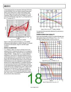
Figure 45 shows data results of the extended dynamic range at
120 MHz with error in VOUT.
1.750
1.625
1.500
1.375
1.250
1.125
1.000
0.875
0.750
0.625
0.500
0.375
0.250
3.0
2.5
2.0
1.5
1.0
0.5
0
–0.5
–1.0
–1.5
–2.0
–2.5
–3.0
V
V
V
+25°C
–40°C
+85°C
OUT
OUT
OUT
ERR0R +25°C
ERR0R –40°C
ERR0R +85°C
–90 –80 –70 –60 –50 –40 –30 –20 –10
0
10
20
P
(dBm)
IN
this results in a 95 dB variation for a 1.5 V change in VOUT
.
Figure 45. Output and Conformance for the AD8368/ADL5513
Extended Dynamic Range Circuit
VPOS
VPOS VPOS1 VPOS2 VPOS3
1nF
5.6pF
GND
VPOS
VPOS
VPOS2
215Ω
INPUT
10nF
0Ω
C7
1000pF
VPSI
VPSI
0.1uF
100pF
INPT
C12
1nF
C15
0.1µF
10nH
VPOS3
ICOM
MODE
VPSI
10kΩ
VPSO
VPSO
OUTP
AD8368
VPOS1
C12
1nF
C15
0Ω
0.1µF
10nF
0Ω
VOUT
VPSI
VPOS
1kΩ
VOUT
TADJ
0.1µF
12
VSET 11
1
OCOM
ENBL
47nF
C10
1nF
2 INHI ADL5513
52.3Ω
3 INLO
COMM 10
BAND-PASS
120MHz
1nF
10nF
VPOS
9
4
1kΩ
VTADJ = 0.89V
100pF
Z1
0.1uF
VPOS
1kΩ
Figure 46. ADL5513 with 95 dB Dynamic Range
Rev. 0 | Page 22 of 28

 ADI [ ADI ]