ADL5513
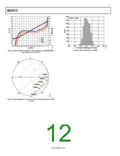
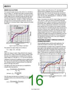
Figure 31 shows a plot of the error at 25°C, the temperature at
which the device is calibrated. Error is not 0 dB over the full
dynamic range. This is because the log amp does not perfectly
follow the ideal VOUT vs. PIN equation, even within its operating
range. The error at the calibrating points of −20 dBm and −40 dBm
is equal to 0 dB by definition.
ERROR CALCULATIONS
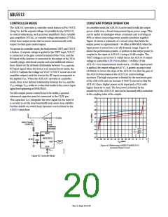
The measured transfer function of the ADL5513 at 100 MHz is
shown in Figure 31. The figure shows plots of measured output
voltage, calculated error, and an ideal line. The input power and
output voltage are used to calculate the slope and intercept values.
The slope and intercept are calculated using linear regression
over the input range from −40 dBm to −20 dBm. The slope and
intercept terms are used to generate an ideal line. The error is
the difference in measured output voltage compared to the ideal
output line.
Figure 31 also shows error plots for output voltages measured at
−40°C and 85°C. These error plots are calculated using slope
and intercept at 25°C, which is consistent in a mass-production
environment, where calibration over temperature is not practical.
This is a measure of the linearity of the device. Error from the
linear response to the CW waveform is not a measure of absolute
accuracy because it is calculated using the slope and intercept of
each device. However, error verifies the linearity of the devices.
Similarly, at temperature extremes, error represents the output
voltage variations from the 25°C ideal line performance. Data
presented in the graphs are the typical error distributions observed
during characterization of the ADL5513. Device performance
was optimized for operation at 85°C; this can be changed by
changing the voltage at TADJ.
2.4
2.2
2.0
1.8
1.6
1.4
1.2
1.0
0.8
0.6
0.4
0.2
0
3.0
IDEAL LINE
2.5
V
V
V
AND ERROR @ +25°C
AND ERROR @ –40°C
AND ERROR @ +85°C
OUT
OUT
OUT
2.0
1.5
1.0
V
OUT1
0.5
0
V
OUT2
–0.5
–1.0
–1.5
–2.0
–2.5
–3.0
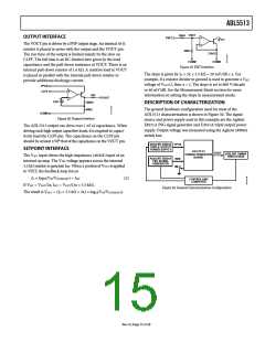
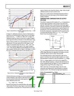
ADJUSTING ACCURACY THROUGH CHOICE OF
CALIBRATION POINTS
P
P
IN1
IN2
Choose calibration points to suit the specific application, but
usually they should be in the linear range of the log amp.
P
(dBm)
IN
Figure 31. Typical Output Voltage vs. Input Signal
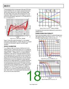
In some applications, very high accuracy is required at a reduced
input range; in other applications, good linearity is necessary over
the full power input range. The linearity of the transfer function
can be adjusted by choice of calibration points. Figure 32 and
Figure 33 show plots for a typical device at 3600 MHz as an exam-
ple of adjusting accuracy through choice of calibration points.
The equation for output voltage can be written as
V
OUT = Slope × (PIN − Intercept)
where:
Slope is the change in output voltage divided by the change in
input power, PIN. Slope is expressed in volts per decibel (V/dB).
Intercept is the calculated power in decibels (dB) at which the
output voltage is 0 V. Note that VOUT = 0 V can never be achieved.
2.50
2.25
2.00
1.75
1.50
1.25
1.00
0.75
0.50
0.25
0
2.5
2.0
1.5
Calibration is performed by applying two known signal levels to
the ADL 5513 and measuring the corresponding voltage outputs.
The calibration points are in general chosen to be within the
linear-in-dB range of the device.
1.0
0.5
0
Calculation of the slope and intercept are accomplished by
using the following equations:
–0.5
–1.0
–1.5
–2.0
–2.5
+25°C
–40°C
+85°C
+125°C
VOUT(MEASURED)1 VOUT(MEASURED)2
Slope
P
IN1 P
IN2
VOUT(MEASURED)
Slope
–70 –65 –60 –55 –50 –45 –40 –35 –30 –25 –20 –15 –10 –5
0
5 10
Intercept PIN1
P
(dBm)
IN
Figure 32. Typical Device at 3600 MHz, Calibration Points at PIN = −20 dBm
and −40 dBm
Once the slope and intercept are calculated, VOUT(IDEAL) can be
calculated, and the error is determined using the following
equation:
(VOUT(MEASURED) VOUT(IDEAL))
Error
Slope
Rev. 0 | Page 16 of 28

 ADI [ ADI ]