ADL5513
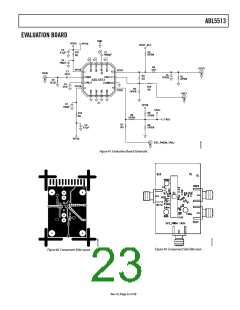
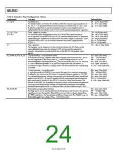
Table 5. Evaluation Board Configuration Options
Component
Function
Default Value
C1, C2, R1
Input interface.
R1 = 52.3 Ω (Size 0402)
C1 = 47 nF (Size 0402)
C2 = 47 nF (Size 0402)
The 52.3 Ω resistor in Position R1 combines with the internal input impedance of
the ADL5513 to give a broadband input impedance of about 50 Ω. C1 and C2 are
dc-blocking capacitors. A reactive impedance match can be implemented by
replacing R1 with an inductor and C1 and C2 with appropriately valued capacitors.
C3, C4, C5, C6,
R11, R12
Power supply decoupling.
C3 = 0.1 µF (Size 0402)
C4 = 100 pF (Size 0402)
C5 = 100 pF (Size 0402)
C6 = 0.1 µF (Size 0402)
R11 = 0 Ω (Size 0402)
R12 = 0 Ω (Size 0402)
The nominal supply decoupling consists of a 100 pF filter capacitor placed
physically close to the ADL5513 and a 0.1 µF capacitor placed nearer to the power
supply input pin. If additional isolation from the power supply is required, a small
resistance (R11 or R12) can be installed between the power supply and the
ADL5513.
C7
Filter capacitor.
C7 = 1000 pF (Size 0402)
The low-pass corner frequency of the circuit that drives the VOUT pin can be
lowered by placing a capacitor between CLPF and ground. Increasing this
capacitor increases the overall rise/fall time of the ADL5513 for pulsed input
signals.
R2, R3 R4, R5, R10, RL, CL Output interface—measurement mode.
In measurement mode, a portion of the output voltage is fed back to the VSET pin via
R2 = open (Size 0402)
R3 = 1 kΩ (Size 0402)
R4 = 0 Ω (Size 0402)
R5 = open (Size 0402)
R10 = open (Size 0402)
RL = CL = open (Size 0402)
R4. The magnitude of the slope of the VOUT output voltage response can be
increased by reducing the portion of VOUT that is fed back to VSET. R3 can be used
as a back-terminating resistor or as part of a single-pole, low-pass filter. If a
reduction in slope is desired, a voltage divider can be installed at the output using
R3 and RL.
Output interface—controller mode.
R2 = open (Size 0402)
R3 = 1 kΩ (Size 0402)
R4 = open (Size 0402)
R5 = open (Size 0402)
R10 = 0 Ω (Size 0402)
RL = CL = open (Size 0402)
In controller mode, the ADL5513 can control the gain of an external component.
To allow for this, remove the R4 resistor. A setpoint voltage is applied to Pin VSET.
The value of this setpoint voltage corresponds to the desired RF input signal level
applied to the ADL5513 RF input. A sample of the RF output signal from this variable
gain component is applied to the ADL5513 input by a directional coupler. The
voltage at the VOUT pin is applied to the gain control of the variable gain element.
The magnitude of the control voltage can optionally be reduced via a voltage
divider comprising R3 and RL, or a low-pass filter can be installed using R3 and CL.
R6, R7, R8, R9
Temperature compensation interface.
R6 = open (Size 0402)
R7 = 0 Ω (Size 0402)
R8 = open (Size 0402)
R9 = open Ω (Size 0402)
A voltage source can be used to optimize the temperature performance for various
input frequencies. The pads for R8 and R9 can be used for a voltage divider from
the VPOS node to set the TADJ voltage at different frequencies. The ADL5513 can be
disabled by applying a voltage of VPOS − 0.3 V to this node.
Rev. 0 | Page 24 of 28

 ADI [ ADI ]