ADL5513
For example, PINTERCEPT for a sinusoidal input signal expressed in
terms of decibels referred to 1 mW (dBm) in a 50 Ω system is
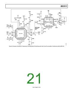
MEASUREMENT MODE
When the VOUT voltage or a portion of the VOUT voltage is fed
back to the VSET pin, the device operates in measurement
mode. As shown in Figure 40, the ADL5513 has an offset
voltage, a positive slope, and a VOUT measurement intercept at
the low end of its input signal range.
P
P
INTERCEPT(dBm) =
INTERCEPT(dBV) – 10 × log10(Z0 × 1 mW/1 Vrms2) =
−100 dBV − 10 × log10(50 × 10−3) = −87 dBm
(7)
Further information on the intercept variation dependence upon
waveform can be found in the AD8313 and AD8307 data sheets.
2.4
2.2
2.0
1.8
1.6
1.4
1.2
1.0
0.8
0.6
0.4
0.2
0
3.0
2.5
SETTING THE OUTPUT SLOPE IN MEASUREMENT
MODE
2.0
1.5
1.0
To operate in measurement mode, VOUT is connected to VSET.
Connecting VOUT directly to VSET yields the nominal
logarithmic slope of approximately 20 mV/dB. The output swing
corresponding to the specified input range is then approximately
0.47 V to 2.0 V. The slope and output swing can be increased by
placing a resistor divider between VOUT and VSET (that is, one
resistor from VOUT to VSET and one resistor from VSET to
ground). The input impedance of VSET is approximately 40 kΩ.
Slope-setting resistors should be kept below 20 kΩ to prevent
this input impedance from affecting the resulting slope. If two
equal resistors are used (for example, 10 kΩ/10 kΩ), theslope
doubles to approximately 40 mV/dB.
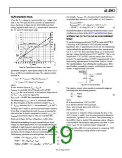
V
ERROR 25°C
OUT1
0.5
0
V
OUT2
–0.5
–1.0
–1.5
–2.0
–2.5
–3.0
V
OUT
IDEAL
V
25°C
OUT
P
P
IN1
IN2
P
(dBm)
IN
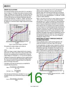
Figure 40. Typical Output Voltage vs. Input Signal
The output voltage vs. input signal voltage of the ADL5513 is
linear-in-dB over a multidecade range. The equation for this
function is
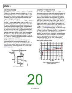
ADL5513
VOUT
40mV/dB
10kΩ
10kΩ
VSET
V
OUT = X × VSLOPE/DEC × log10(VIN/VINTERCEPT) =
X × VSLOPE/dB × 20 × log10(VIN/VINTERCEPT
where:
X is the feedback factor in VSET = VOUT/X.
)
(3)
Figure 41. Increasing the Slope
The required resistor values needed to increase the slope are
calculated from the following equation.
V
V
SLOPE/DEC is nominally 400 mV/decade or 20 mV/dB.
INTERCEPT is the x-axis intercept of the linear-in-dB portion of
R1
R2
Slope2
Slope1
the VOUT vs. PIN curve (see Figure 40).
+1 =
(8)
VINTERCEPT is −100 dBV for a sinusoidal input signal.
where:
An offset voltage, VOFFSET, of 0.47 V is internally added to
the detector signal, so that the minimum value for VOUT is
X × VOFFSET; therefore, for X = 1, the minimum VOUT is 0.47 V.
R1 is the resistor from VOUT to VSET.
R2 is the resistor from VSET to ground.
Slope1 is the nominal slope of the ADL5513.
Slope2 is the new slope.
The slope is very stable vs. process and temperature variation.
When Base 10 logarithms are used, VSLOPE/DEC represents the
volts per decade. A decade corresponds to 20 dB; VSLOPE/DEC/20 =
It is important to remember when increasing the slope of the
ADL5513 that R1 and R2 must be properly sized so the output
current drive capability is not exceeded. The dynamic range of
the ADL5513 may be limited if the maximum output voltage is
achieved before the maximum input power is reached. In cases
where VPOS is 5 V, the maximum output voltage is 4.7 V.
V
SLOPE/dB represents the slope in volts per decibel (V/dB).
As shown in Figure 40, VOUT voltage has a positive slope.
Although demodulating log amps respond to input signal
voltage, not input signal power, it is customary to discuss the
amplitude of high frequency signals in terms of power. In this
case, the characteristic impedance of the system, Z0, must be
known to convert voltages to their corresponding power levels.
The following equations are used to perform this conversion:
The slope of the ADL5513 can be reduced by connecting VSET
to VOUT and adding a voltage divider on the output.
P(dBm) = 10 × log10(Vrms2/(Z0 × 1 mW))
P(dBV) = 20 × log10(Vrms/1 Vrms
P(dBm) = P(dBV) − 10 × log10(Z0 × 1 mW/1 Vrms
(4)
)
(5)
(6)
2
)
Rev. 0 | Page 19 of 28

 ADI [ ADI ]