ADL5513
1.5
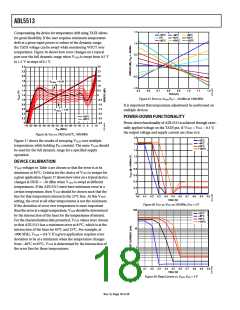
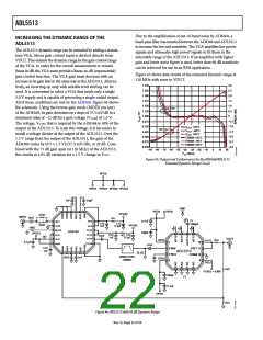
Compensating the device for temperature drift using TADJ allows
for great flexibility. If the user requires minimum temperature
drift at a given input power or subset of the dynamic range,
the TADJ voltage can be swept while monitoring VOUT over
temperature. Figure 36 shows how error changes on a typical
part over the full dynamic range when VTADJ is swept from 0.5 V
to 1.2 V in steps of 0.1 V.
+25°C
0°C
+85°C
–40°C
+45°C
+105°C
–20°C
+65°C
+125°C
1.0
0.5
0
2.4
2.2
2.0
1.8
1.6
1.4
1.2
1.0
0.8
0.6
0.4
0.2
0
3.0
2.5
2.0
–0.5
1.5
V
= 0.5V
TADJ
1.0
–1.0
0.5
0.5
0.6
0.7
0.8
0.9
1.0
1.1
1.2
TADJ (V)
0
Figure 37. Error vs. VTADJ, PIN = −30 dBm at 1900 MHz
–0.5
–1.0
–1.5
–2.0
–2.5
–3.0
It is important that temperature adjustment be performed on
multiple devices.
V
= 1.2V
TADJ
+25°C
+85°C
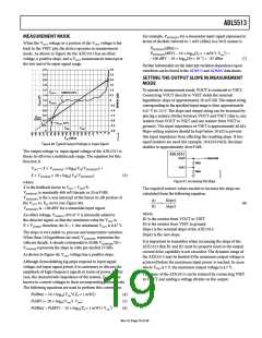
POWER-DOWN FUNCTIONALITY
Power-down functionality of ADL5513 is achieved through exter-
nally applied voltage on the TADJ pin. If VTADJ = VPOS − 0.3 V,
the output voltage and supply current are close to 0.
–70 –65 –60 –55 –50 –45 –40 –35 –30 –25 –20 –15 –10 –5
0
5 10
P
(dBm)
IN
Figure 36. VOUT vs. TADJ at 85°C, 1900 MHz
1.8
+25°C
Figure 37 shows the results of sweeping VTADJ over multiple
temperatures while holding PIN constant. The same VTADJ should
be used for the full dynamic range for a specified supply
operation.
–40°C
+85°C
+125°C
1.6
1.4
1.2
1.0
0.8
0.6
0.4
0.2
0
DEVICE CALIBRATION
VTADJ voltages in Table 4 are chosen so that the error is at its
minimum at 85°C. Criteria for the choice of VTADJ is unique for
a given application. Figure 37 shows how error on a typical device
changes at INHI = −30 dBm when VTADJ is swept at different
temperatures. If the ADL5513 must have minimum error at a
certain temperature, then VTADJ should be chosen such that the
line for that temperature intersects the 25°C line. At this VTADJ
setting, the error at all other temperatures is not the minimum.
If the deviation of error over temperature is more important
than the error at a single temperature, VTADJ should be determined
by the intersection of the lines for the temperatures of interest.
For the characterization data presented, VTADJ values were chosen
so that ADL5513 has a minimum error at 85°C, which is at the
intersection of the lines for 85°C and 25°C. For example, at
1900 MHz, VTADJ = 0.8 V. If a given application requires error
deviation to be at a minimum when the temperature changes
from −40°C to 85°C, VTADJ is determined by the intersection of
the error line for those temperatures.
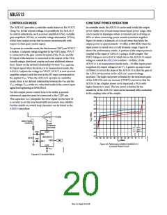
4.0
4.1
4.2
4.3
4.4
4.5
4.6
4.7
4.8
4.9
5.0
TADJ (V)
Figure 38. VOUT vs. VTADJ at 100 MHz, VPOS = 5 V
100
10
1
+25°C
–40°C
+85°C
+125°C
0.1
4.0
4.1
4.2
4.3
4.4
4.5
4.6
4.7
4.8
4.9
5.0
TADJ (V)
Figure 39. Sleep Current vs. VTADJ, VPOS = 5 V
Rev. 0 | Page 18 of 28

 ADI [ ADI ]