ADL5513
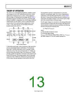
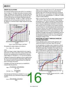
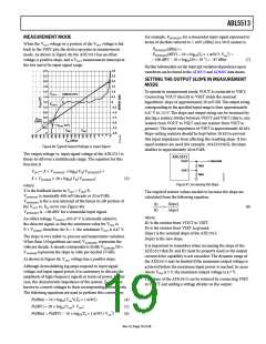
VSET
20kΩ
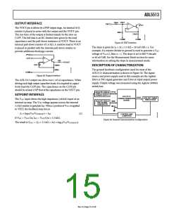
OUTPUT INTERFACE
VSET
I
SET
The VOUT pin is driven by a PNP output stage. An internal 10 Ω
resistor is placed in series with the output and the VOUT pin.
The rise time of the output is limited mainly by the slew on
CLPF. The fall time is an RC-limited slew given by the load
capacitance and the pull-down resistance at VOUT. There is an
internal pull-down resistor of 1.6 kΩ. A resistive load at VOUT
is placed in parallel with the internal pull-down resistor to
provide additional discharge current.
20kΩ
3.5kΩ
COMM
COMM
Figure 29. VSET Interface
The slope is given by ID × 2x × 3.5 kΩ = 20 mV/dB × x. For
example, if a resistor divider to ground is used to generate a VSET
voltage of VOUT/2, then x = 2. The slope is set to 800 V/decade
or 40 mV/dB. See the Measurement Mode section for more
information on setting the slope in measurement mode.
VPOS
CLPF
10Ω
VOUT
+
0.8V
1200Ω
400Ω
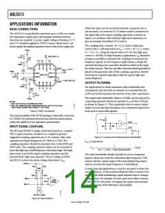
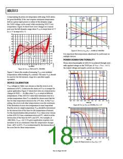
DESCRIPTION OF CHARACTERIZATION
–
The general hardware configuration used for most of the
ADL5513 characterization is shown in Figure 30. The signal
source and power supply used in this example are the Agilent
E8251A PSG signal generator and E3631A triple output power
supply. Output voltage was measured using the Agilent 34980A
switch box.
COMM
Figure 28. Output Interface
The ADL5513 output can drive over 1 nF of capacitance. When
driving such high output capacitive loads, it is required to capaci-
tively load the CLPF pin. The capacitance on the CLPF pin
should be at least 1/50th that of the capacitance on the VOUT pin.
AGILENT E3631A
TRIPLE OUTPUT
POWER SUPPLY
VPOS
SETPOINT INTERFACE
ADL5513
CHARACTERIZATION
BOARD
VOUT
AGILENT 34980A
SWITCH BOX
The VSET input drives the high impedance (40 kΩ) input of an
internal op amp. The VSET voltage appears across the internal
3.5 kΩ resistor to generate ISET. When a portion of VOUT is applied
to VSET, the feedback loop forces
AGILENT E8251A
PSG SIGNAL
GENERATOR
INHI
INLO
ID × log10(VIN/VINTERCEPT) = ISET
(2)
CONTROLLING
COMPUTER
If VSET = VOUT/2x, ISET = VOUT/(2x × 3.5 kΩ).
The result is VOUT = (ID × 3.5 kΩ × 2x) × log10(VIN/VINTERCEPT).
Figure 30. General Characterization Configuration
Rev. 0 | Page 15 of 28

 ADI [ ADI ]