ADL5513
THEORY OF OPERATION
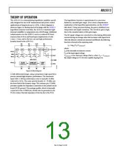
The ADL5513 is a demodulating logarithmic amplifier, specifi-
cally designed for use in RF measurement and power control
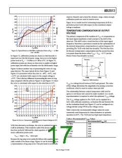
applications at frequencies up to 4 GHz. A block diagram is
shown in Figure 24. Sharing much of its design with the AD8313
logarithmic detector/controller, the ADL5513 maintains tight
intercept variability vs. temperature over a 80 dB range. Additional
enhancements over the AD8313, such as a reduced RF burst
response time of 20 ns and board space requirements of only
3 mm × 3 mm, add to the low cost and high performance
benefits found in the ADL5513.
The logarithmic function is approximated in a piecewise
fashion by cascaded gain stages. (For a more comprehensive
explanation of the logarithm approximation, see the AD8307
data sheet.) Using precision biasing, the gain is stabilized over
temperature and supply variations. The overall dc gain is high,
due to the cascaded nature of the gain stages.
The RF signal voltages are converted to a fluctuating differential
current having an average value that increases with signal level.
After the detector currents are summed and filtered, the following
function is formed at the summing node:
NC
NC
CLPF
NC
ID × log10(VIN/VINTERCEPT
where:
ID is the internally set detector current.
VIN is the input signal voltage.
)
(1)
16
15
14
13
12
11
DET
DET
DET
DET
DET
I
V
VOUT
VSET
1
VPOS
INHI
2
3
I
V
VINTERCEPT is the intercept voltage (that is, when VIN = VINTERCEPT,
INLO
the output voltage is 0 V, if it were capable of going to 0).
ADL5513
10 COMM
VPOS
4
SLOPE
CONTROL
BAND GAP
REFERENCE
GAIN
BIAS
9
TADJ
5
6
7
8
NC
NC
NC
NC
Figure 24. Block Diagram
A fully differential design, using a proprietary, high speed SiGe
process, extends high frequency performance. The maximum
input with 1 dB log conformance error is typically 10 dBm
(referred to 50 Ω). The noise spectral density of −70 dBm sets
the lower limit of the dynamic range. The common pin, COMM,
provides a quality low impedance connection to the printed circuit
board (PCB) ground. The package paddle, which is internally
connected to the COMM pin, should also be grounded to the
PCB to reduce thermal impedance from the die to the PCB.
Rev. 0 | Page 13 of 28

 ADI [ ADI ]