AD9807/AD9805
is inverted and amplified by the PGA; the setting in the corre-
sponding PGA Gain Register determines the gain of the PGA.
T he output from the PGA is then routed through a high speed
multiplexer to a 12-bit A/D converter (10-bit for AD9805) for
digitization; the multiplexer does cycle in this mode. After
digitization, the data is modified by the amount indicated in
the Even Offset Registers. A digital subtracter allows additional
pixel rate offset modification of the signal based on the values
written to the OFFSET data bus. Finally, a digital multiplier
allows pixel rate gain modification of the signal based on the
values written to the GAIN data bus. Latency is 6 ADCCLK
cycles (7 cycles for the gain and offset bus; see Figure 14).
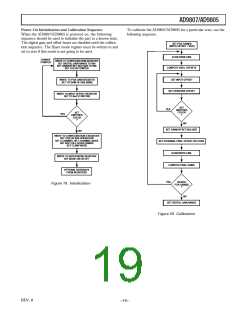
T his feature has been included to accommodate the use of the
part with an area CCD (Bayer Mode). T he mode is initiated by
writing a one to the LSB of the register at Address 7 (see Figure
21). T he write to enable the mode should be performed when
the STRTLN input is inactive (low) and the ADCCLK is running.
T he first pixel after an active edge on ST RT LN will be a green
pixel. All pixels in Bayer Mode are even and use the even offset
registers. The line will continue alternating GRGRGR pixels
until ST RT LN goes inactive. T he next line will be BGBGBG
pixels (the first pixel after the active ST RT LN edge being blue).
Line type will then alternate between GRGRGR and BGBGBG
type. T o reset the next line to GRGRGR type at the start of the
next frame/image, rewrite the Bayer mode enable bit to a one
during the inactive ST RT LN period. All red and blue pixels
pass through the blue channel of the part and use the blue PGA
and offset registers. T o use a different offset/PGA gain value the
register must be written to between lines. Green pixels on either
line type pass through the green channel.
T he state of ST RT LN is evaluated on the rising edges of
ADCCLK. When ST RT LN is low, the internal circuitry is
reset on the next rising edge of ADCCLK; the odd/even
circuitry is configured to expect even pixels.
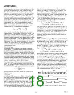
ADCCLK
tOD
DATA<11:0>
tHZ
tEDV
OEB
Figure 11. Digital Output Tim ing
PIXEL n
PIXEL n+1
PIXEL n+2
RIN, GIN, BIN
CDSCLK1
CDSCLK2
ADCCLK
R, G, B
R, G, B
R, G, B
R
G
B
R
G
B
R
G
B
DATA<11:0>
R (n–2)
G (n–2)
B (n–2)
R (n–1)
G (n–1)
B (n–1)
R (n)
GAIN<n:0>
GAIN<m:0>
R (n)
G (n)
B (n)
R (n+1)
G (n+1)
B (n+1)
R (n+2)
G (n+2)
B (n+2)
R (n+3)
Figure 12. DOUT Latency, 3-Channel CDS Mode
REV. 0
–15–

 ADI [ ADI ]