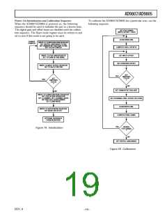
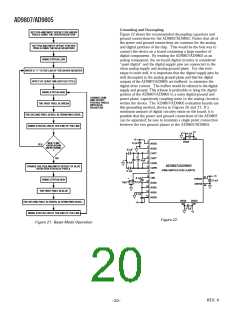
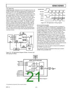
AD9807/AD9805
Calculating O ver all Gain
where GAIN<n:0> is the decimal representation of the GAIN
bus data bits, Y = 4096 for the AD9807, Y = 1024 for the
AD9805, and X equals 1, 3 or 7 depending on Bits 0–2 in the
Configuration Register.
T he overall gain for the AD9807/AD9805 can accommodate a
wide range of input voltage spans. T he total gain is a composite
of analog gain (from the PGAs), digital gain (from the digital
multiplier) and the input span setting for the A/D (2 V or 4 V). T o
determine the overall gain setting for the AD9807/AD9805, always
multiply the PGA gain setting by the digital gain setting. In
addition, the 2 V/4 V reference option can effectively provide
analog gain for input signals less than 2 V p-p.
O ver all Tr ansfer Function
T he overall transfer function for the AD9807 can be calculated
as follows:
V
(
± InputOffset × PGA Gain
)
IN
[
]
ADCOUT
=
× 4096
2 ×VREF
Overall Gain = Analog Gain × Digital Gain
For example, with the PGA gain equal to 1 (gain setting equals
all “zeros”) and the digital multiplier equal to 1, the minimum
gain equals 1. With these settings, input signals can be as large
as 2 V or 4 V depending on the reference setting. Alternatively,
with the PGA gain equal to 4 (gain setting equals all “ones”)
and the digital multiplier equal to 8, the maximum gain equals
32. With the A/D reference span set to 2 V, an input signal span
as small as 62.5 mV p-p will produce a digital output spanning
from all “zeros” to all “ones.” For ranges between 62.5 mV and
4 V, see the Digital Gain and Analog Gain sections of the data
sheet.
DOUT = [ADCOUT + Offset Register – Offset Bus][Digital Gain]
Choosing the Input Coupling Capacitor s
Because of the dc offset present at the output of CCDs, it is likely
that these outputs will require some form of dc restoration to be
compatible with the input requirements of the AD9807/AD9805.
T o simplify input level shifting, a dc blocking capacitor may be
used in conjunction with the internal biasing circuits of the
AD9807/AD9805 to accomplish the necessary dc restoration.
Figure 17 shows the equivalent analog input for the VINR,
VING and VINB inputs.
Analog Gain
T he transfer function of the PGA is:
4
AD9807/AD9805
Analog Input =
15 − x
4pF
1 + 3 ×
I
C
BIAS
S1
15
V
IN
CDS
CDSCLK1
STRTLN
where x is the decimal representation of the settings in the PGA
gain register. Figure 16 shows the graph of this transfer
function on both a linear and logarithmic scale. T he transfer
function is approximately linear in dB.
4pF
5kΩ
CONFIG
REG 2<7>
V
BIAS
4.0
12
CONFIG
REG 2<0>
CONFIG
REG 2<6>
3.5
10
CDSCLK2
3.0
2.5
2.0
1.5
1.0
8
6
4
2
0
GAIN (dB)
Figure 17. Equivalent Analog Inputs (VINR, VING, and
VINB)
GAIN
Enabling CDS functionality and Line Clamp Mode with Bits 0,
6 and 7 in Configuration Register 2 allows switch S1 to turn on
when STRTLN is low and CDSCLK1 goes high. This connects
a 5 kΩ biasing resistor to the inputs. T his arrangement acts to
bias the average level of the input signal at voltage, VBIAS. T he
voltage, VBIAS, changes depending on the selected PGA gain set-
ting. Specifically, for gain settings from 0 to 5, VBIAS equals 4 V;
for gain settings from 10 to 15, VBIAS equals 3 V. For gain set-
tings between 5 and 10, VBIAS decreases linearly from 4 V to 3 V.
0
1
2
3
4
5
6
7
8
9
10 11 12 13 14 15
PGA GAIN SETTING
Figure 16. PGA Transfer Function
D igital Gain
T he digital multiplier section of the AD9807/AD9805 allows the
user to apply gain in addition to that afforded by the analog
PGA. T he minimum gain of the digital multiplier is always 1.
T he user sets the maximum gain of the digital multiplier to be 8,
4, or 2 with Bits 0–2 in the Configuration Register. (T he max
gain is the same for all three channels.) T he digital gain
applied to the output from the digital subtracter is calculated
using the equation:
T he size of the coupling capacitor is dependent on several
factors including signal swing, allowable droop, and acquisition
time. T he following procedure shows how to determine the
recommended range of capacitors.
Calculating C MAX
T he maximum capacitor value is largely dependent on the
degree of accuracy and how quickly the input signal must be
level-shifted into the valid input range of the degree of accuracy.
Other factors affecting the speed of the capacitor charging or
Gain < n:0 >
Digital Gain = 1+
× X
Y
REV. 0
–17–

 ADI [ ADI ]