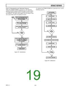
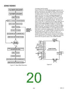
AD9807/AD9805
discharging include the amount of time that input switch S1 is
turned on, the input impedance of the AD9807/AD9805 and
the output impedance of the circuit driving the coupling
capacitor. T he impedance of the drive circuit, ROUT , the input
impedance of the AD9807/AD9805, RIN, and the desired
charging time, tACQ, are all known quantities. Note that tACQ
may not necessarily occur over a continuous period of time; it may
actually be an accumulation of discrete charging periods. T his
is typical where CDSCLK1 is asserted only during the reset
levels of the pixels. In this case, the quantity, m × T , may be
substituted for tACQ, where m is the number of periods
CDSCLK1 is asserted and T is the period of the assertion.
Given these quantities, the maximum value for the input
coupling capacitor is computed from the equation:
With dV = 1.2 volts, a clamp accuracy of 100 mV should be
sufficient (VE =100 mV), but this value can be adjusted. T he
amount of time available to charge up the input capacitor,
T
ACQ, will equal the period of CDSCLK1 (when the clamp
switch is closed) times the number of optical black pixels. With
a pixel rate of 2 MHz, CDSCLK1 would typically be around
100 ns wide, giving TACQ =1800 ns or
1.8 µs. T he input impedance of the AD9807 is 5K, and the
input bias current is 10 nA. Assume the source impedance
driving the AD9807 is low (ROUT = 0).
CMAX = (1.8 µs/5K) × (1/ln (1.5/0.1)) = 133 pF
CMIN = (10 nA/1.2) × 5000 × 500 ns = 21 pF
Note that a capacitor larger than 133 pF would still work, it
would just take several lines to charge the input capacitor up
to the full VC level. Another option to lengthen TACQ is by
clocking the CCD and CDSCLK1 while the transport motor
moves the scanner carriage. T his would extend TACQ to
several hundred µs or more, meaning that only very fine
adjustment would be needed during the limited number of
optical black pixels.
tACQ
VC
VE
CMAX
/ln
RIN + ROUT
where VC is the required voltage change across the coupling
capacitor and VE is the maximum tolerable error voltage. VC is
calculated by taking the difference between the CCD’s reset
level and the internal bias level of the AD9807/AD9805. VE is
the level of accuracy to which the input capacitor must be charged
and is system dependent. Usually the allowable droop of the
capacitor voltage is taken into account. T his is discussed below.
For example, if the CCD output can droop up to 1 volt without
affecting the accuracy of the CDS, then clamping to within
about one tenth of the allowable droop (100 mV) should be
sufficient in most cases.
Exa m ple 2
A 7926 pixel CCD running at 2 MHz has a reset level of 6 volts,
an output voltage of 2.9 volts and 80 optical black pixels. Using
the AD9807 with an input span of 4 volts and a PGA gain of
1.25, VBIAS = 4 volts. T he maximum required voltage change
on the capacitor, VC, is 2 volts and the maximum amount of
droop dV for one line is 1.1 volts. T ACQ will be 80 × 100 ns or 8
µs, and VE = 100 mV should be sufficient. Again, RIN = 5K,
ROUT = 0, and IBIAS = 10 nA.
Calculating C MIN
Determining CMIN is a function of the amount of allowable
voltage droop. It is important that the signals at the inputs of
the AD9807/AD9805 remain within the supply voltage limits so
the CDSs are able to accurately digitize the difference between
the reset level and the video level. Assuming the input voltages
are initially biased at the correct levels, the input bias current of
the AD9807/AD9805 inputs will discharge the input coupling
capacitors resulting in voltage droop. After taking into account
any droop, the peaks of the input signal must remain within the
required voltage limits of AD9807/AD9805 inputs.
CMAX = (8 µs/5K) × (1/ln (2/0.1)) 534 pF
CMIN = (10 nA/1.1) × (7926) × (500 ns) = 36 pF
Again, a larger capacitor may be used if several lines are allowed
for to initially charge up the cap, or if the CCD and CDSCLK1
are clocked during the moving of the scanner carriage.
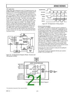
Gener ating 3-Channel Tim ing fr om a 16 ؋
Master Clock
Generating the required signals for CDSCLK1, CDSCLK2 and
ADCCLK is easily accomplished with a master clock running
16 × the desired per channel pixel rate (i.e., 2 MSPS pixel rate
requires 32 MH z master clock). T he timing diagram shown
in Figure 18 meets all the minimum and maximum timing
specifications. Note that a 16 × master clock using only rising
edges was chosen instead of using both edges of an 8 × rate
clock to ensure immunity to duty cycle variations.
Specifically, CMIN is a function of the maximum allowable
droop, dV, in one scan line, the number of pixels across one scan
line, n, the period of one pixel, t, and the input bias current of
the AD9807/AD9805, IBIAS. CMIN is calculated from the equation:
IBIAS
CMIN
=
× n × t
dV
500ns
Some examples are given below showing the typical range of
capacitor values.
MASTER
1
2
3
4
5
6
7
8
9
10
11 12
13 14
15
16
(32MHz)
CDSCLK1
CDSCLK2
Exa m ple 1
A 5000 pixel CCD running at a 2 MHz (t = 500 ns) has a reset
level of 4.5 volts and an output voltage of 1.8 volts. T he number
of optical black pixels available at the start of a line is 18. Using
the AD9807/AD9805 with an input span of 4 volts and a PGA
gain of 2 gives a VBIAS of 3 volts. If the input signal is clamped
to 3 volts during the optical black pixels, the required voltage
change on the input capacitor, VC, equals (4.5 – 3) or 1.5 volts
and the maximum droop allowable during one line, dV, will be
(3 – 1.8) or 1.2 volts before the signal droops below 0 volts.
ADCCLK
Figure 18. Tim ing Schem e Using 16 × Master Clock
REV. 0
–18–

 ADI [ ADI ]