AD9807/AD9805
Input O ffset Register s
Color P ointer
T he Input Offset Registers control the amount of analog offset
applied to the analog inputs prior to the PGA portion of the
AD9807/AD9805; there is one Input Offset Register for each
color. Figure 8 shows the Input Offset Register format. T he
offset range may be varied between –80 mV and 20 mV. T he
data format for the Input Offset Registers is straight binary
coding. An all “zeros” data word corresponds to –80 mV. An
all “ones” data word corresponds to 20 mV. T he offset is
variable in 256 steps. T he contents of the color pointer in the
Configuration Register at the time an Input Offset Register is
written indicates the color for which that offset setting applies.
Both the AD9807 and the AD9805 use Bits 6 and 7 in the
Configuration Register to direct data to the corresponding
internal registers. T able III shows the mapping of Bits 6 and 7
to their corresponding color.
Table III. Color P ointer Map
Bit 7
Bit 6
Color Register
0
0
1
1
0
1
0
1
Red
Green
Blue
RESERVED
7
6
5
4
3
2
1
0
Configur ation Register 2
Configuration Register 2 controls several functions: color/black
and white selection, CDS enabling, A/D Reference Control
and Input Clamp Mode. Figure 7 shows the AD9807 and
AD9805 Configuration Register 2 format. Setting Bit 0 enables
the three internal CDS blocks of the AD9807/AD9805. Reset-
ting Bit 0 disables the internal CDS blocks, configuring the part
for SHA operation. Setting Bit 1 places the AD9807/AD9805 in
single-channel (black & white) mode. In this mode, only one of
the three input channels is used. T he color bits in the configu-
ration register at the time of the last write indicate the particular
channel used. Resetting Bit 1 places the AD9807/AD9805 in
color mode and all three input channels are enabled. Bits 2-4
control the full-scale input span of the A/D. Setting Bit 2 results in
a 4 V p-p input span. Setting Bit 3 results in a 2 V p-p full-scale
input span. Setting Bit 4 results in a full-scale span set by an
external reference connected to the VREF pin of the AD9807/
AD9805 (Full Scale = 2 × VREF). Resetting Bits 2, 3 or 4
disables that particular mode. Bits 6 and 7 select the desired
clamp mode (see Figure 17). T able IV shows the truth table
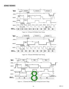
for clamp mode functionality. Line clamp mode allows control
of the input switch (S1) via CDSCLK1 only while ST RT LN is
reset. Pixel clamp mode allows control of the input switch (S1)
via CDSCLK1 regardless of the state of ST RT LN. No clamp
mode disables the input switch (S1) regardless of the selected
mode of CDS operation.
ANALOG OFFSET (LSB)
ANALOG OFFSET
ANALOG OFFSET
ANALOG OFFSET
ANALOG OFFSET
ANALOG OFFSET
ANALOG OFFSET
ANALOG OFFSET (MSB)
Figure 8. Input Offset Registers Form at
P GA Gain Register s
Bits 0–3 of the PGA Gain Registers control the amount of gain
applied to the analog inputs prior to the A/D conversion
portion of the AD9807/AD9805; there is one PGA Gain
Register for each channel. Figure 9 shows the PGA Gain Register
format. T he gain range may be varied between 1 and 4. T he
data format for the PGA Gain Registers is straight binary
coding. An all “zeros” data word corresponds to an analog
gain of 1. An all “ones” data word corresponds to an analog
gain of 4. T he gain is variable in 16 steps (see Figure 16).
T he contents of the color pointer in the Configuration
Register at the time a PGA Gain Register is written indicates
the color for which that gain setting applies. Bits 4–7 of the PGA
Gain Registers are reserved.
7
6
5
4
3
2
1
0
Table IV. Clam p Mode Truth Table
Bit 7
Bit 6
Clam p Mode
0
0
1
1
0
1
0
1
Line Clamp
Pixel Clamp
No Clamp
PGA0
PGA1
PGA2
PGA3
RESERVED
RESERVED
RESERVED
RESERVED
RESERVED
7
6
5
4
3
2
1
0
Figure 9. PGA Gain Registers Form at
O dd, Even O ffset Register s
CDSEN
BLACK & WHITE
T he Odd and Even Offset Registers provide a means of digitally
compensating the odd and even offset error (Register Imbal-
ance) typical of multiplexed CCD imagers; there is one Odd
and one Even Offset Register for each color. Figure 10 shows
the AD9807/AD9805 Odd and Even Offset Register Formats.
T he data format for the Odd and Even Offset Registers is twos
complement. T he offsets may be varied between positive
ADC FULL SCALE = 4V
ADC FULL SCALE = 2V
EXTERNAL REFERENCE
SET TO 0
CLAMP MODE SELECT
CLAMP MODE SELECT
Figure 7. AD9807/AD9805 Configuration Register 2 Form at
–12–
REV. 0

 ADI [ ADI ]