Data Sheet
AD9653
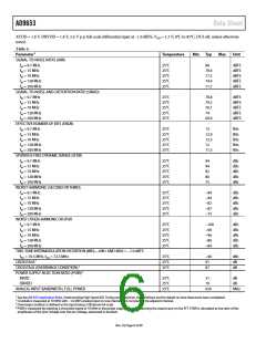
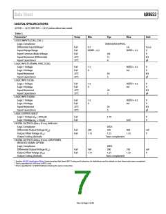
DIGITAL SPECIFICATIONS
AVDD = 1.8 V, DRVDD = 1.8 V, unless otherwise noted.
Table 5.
Parameter1
Temp
Min
Typ
Max
Unit
CLOCK INPUTS (CLK+, CLK−)
Logic Compliance
CMOS/LVDS/LVPECL
Differential Input Voltage2
Input Voltage Range
Input Common-Mode Voltage
Input Resistance (Differential)
Input Capacitance
Full
Full
Full
25°C
25°C
0.2
AGND − 0.2
3.6
AVDD + 0.2
V p-p
V
V
kΩ
pF
0.9
15
4
LOGIC INPUTS (PDWN, SYNC, SCLK)
Logic 1 Voltage
Logic 0 Voltage
Full
Full
1.2
0
AVDD + 0.2
0.8
V
V
Input Resistance
Input Capacitance
25°C
25°C
30
2
kΩ
pF
LOGIC INPUT (CSB)
Logic 1 Voltage
Logic 0 Voltage
Full
Full
1.2
0
AVDD + 0.2
0.8
V
V
Input Resistance
Input Capacitance
25°C
25°C
26
2
kΩ
pF
LOGIC INPUT (SDIO)
Logic 1 Voltage
Logic 0 Voltage
Full
Full
1.2
0
AVDD + 0.2
0.8
V
V
Input Resistance
Input Capacitance
25°C
25°C
26
5
kΩ
pF
LOGIC OUTPUT (SDIO)3
Logic 1 Voltage (IOH = 800 μA)
Logic 0 Voltage (IOL = 50 μA)
DIGITAL OUTPUTS (D0 x, D1 x), ANSI-644
Logic Compliance
Full
Full
1.79
V
V
0.05
LVDS
Differential Output Voltage (VOD)
Output Offset Voltage (VOS)
Output Coding (Default)
Full
Full
290
1.15
345
1.25
400
1.35
mV
V
Twos complement
DIGITAL OUTPUTS (D0 x, D1 x), LOW POWER,
REDUCED SIGNAL OPTION
Logic Compliance
LVDS
Differential Output Voltage (VOD)
Output Offset Voltage (VOS)
Output Coding (Default)
Full
Full
160
1.15
200
1.25
230
1.35
mV
V
Twos complement
1 See the AN-835 Application Note, Understanding High Speed ADC Testing and Evaluation, for definitions and for details on how these tests were completed.
2 This is specified for LVDS and LVPECL only.
3 This is specified for 13 SDIO/OLM pins sharing the same connection.
Rev. 0 | Page 7 of 40

 ADI [ ADI ]