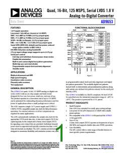
Data Sheet
AD9653
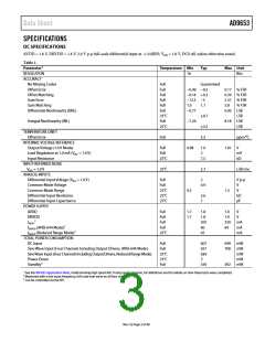
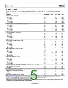
SPECIFICATIONS
DC SPECIFICATIONS
AVDD = 1.8 V, DRVDD = 1.8 V, 2.0 V p-p full-scale differential input at −1.0 dBFS; VREF = 1.0 V, DCS off, unless otherwise noted.
Table 1.
Parameter1
Temperature Min
Typ
Max Unit
RESOLUTION
16
Bits
ACCURACY
No Missing Codes
Offset Error
Offset Matching
Gain Error
Gain Matching
Differential Nonlinearity (DNL)
Full
Guaranteed
Full
Full
Full
Full
Full
25°C
Full
25°C
−0.49 −0.3
−0.14 +0.2
−12.3 −5
0.17 % FSR
0.39 % FSR
2.37 % FSR
1.0
−0.77
1.1
0.7
3.5
3.5
5.8
% FSR
0.95 LSB
LSB
8.18 LSB
LSB
Integral Nonlinearity (INL)
−7.26
TEMPERATURE DRIFT
Offset Error
Full
ppm/°C
INTERNAL VOLTAGE REFERENCE
Output Voltage (1.0 V Mode)
Load Regulation at 1.0 mA (VREF = 1.0 V)
Input Resistance
Full
Full
25°C
0.98
1.0
2
7.5
1.01
V
mV
kΩ
INPUT-REFERRED NOISE
VREF = 1.0 V
25°C
2.7
LSB rms
ANALOG INPUTS
Differential Input Voltage (VREF = 1.0 V)
Common-Mode Voltage
Common-Mode Range
Differential Input Resistance
Differential Input Capacitance
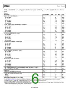
POWER SUPPLY
Full
Full
25°C
25°C
25°C
2
0.9
V p-p
V
V
kΩ
pF
0.5
1.3
2.6
7
AVDD
Full
Full
Full
Full
25°C
1.7
1.7
1.8
1.8
305
60
1.9
1.9
330
64
V
V
mA
mA
mA
DRVDD
2
IAVDD
IDRVDD (ANSI-644 Mode)2
IDRVDD (Reduced Range Mode)2
45
TOTAL POWER CONSUMPTION
DC Input
Full
Full
25°C
25°C
Full
607
657
630
2
649
708
mW
mW
mW
mW
mW
Sine Wave Input (Four Channels Including Output Drivers, ANSI-644 Mode)
Sine Wave Input (Four Channels Including Output Drivers, Reduced Range Mode)
Power-Down
Standby3
356
392
1 See the AN-835 Application Note, Understanding High Speed ADC Testing and Evaluation, for definitions and for details on how these tests were completed.
2 Measured with a low input frequency, full-scale sine wave on all four channels.
3 Can be controlled via the SPI.
Rev. 0 | Page 3 of 40

 ADI [ ADI ]